


Basic Electronics - JFET
The JFET is abbreviated as Junction Field Effect Transistor. JFET is just like a normal FET. The types of JFET are n-channel FET and P-channel FET. A p-type material is added to the n-type substrate in n-channel FET, whereas an n-type material is added to the ptype substrate in p-channel FET. Hence it is enough to discuss one type of FET to understand both.
N-Channel FET
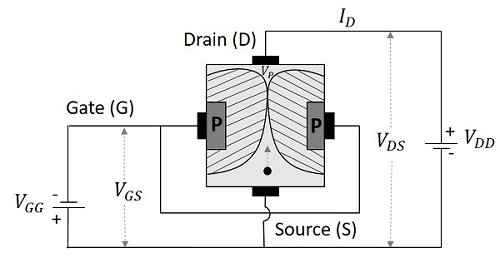
The N-channel FET is the mostly used Field Effect Transistor. For the fabrication of Nchannel FET, a narrow bar of N-type semiconductor is taken on which P-type material is formed by diffusion on the opposite sides. These two sides are joined to draw a single connection for gate terminal. This can be understood from the following figure.
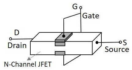
These two gate depositions (p-type materials) form two PN diodes. The area between gates is called as a channel. The majority carriers pass through this channel. Hence the cross sectional form of the FET is understood as the following figure.
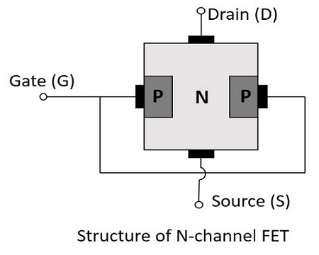
Ohmic contacts are made at the two ends of the n-type semiconductor bar, which form the source and the drain. The source and the drain terminals may be interchanged.
Operation of N-channel FET
Before going into the operation of the FET one should understand how the depletion layers are formed. For this, let us suppose that the voltage at gate terminal say VGG is reverse biased while the voltage at drain terminal say VDDis not applied. Let this be the case 1.
- In case 1, When VGG is reverse biased and VDD is not applied, the depletion regions between P and N layers tend to expand. This happens as the negative voltage applied, attracts the holes from the p-type layer towards the gate terminal.
- In case 2, When VDD is applied (positive terminal to drain and negative terminal to source) and VGG is not applied, the electrons flow from source to drain which constitute the drain current ID.
Let us now consider the following figure, to understand what happens when both the supplies are given.
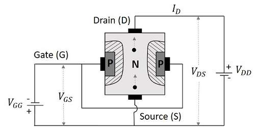
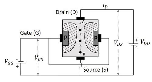
The supply at gate terminal makes the depletion layer grow and the voltage at drain terminal allows the drain current from source to drain terminal. Suppose the point at source terminal is B and the point at drain terminal is A, then the resistance of the channel will be such that the voltage drop at the terminal A is greater than the voltage drop at the terminal B. Which means,
VA>VB
Hence the voltage drop is being progressive through the length of the channel. So, the reverse biasing effect is stronger at drain terminal than at the source terminal. This is why the depletion layer tends to penetrate more into the channel at point A than at point B, when both VGG and VDD are applied. The following figure explains this.
Now that we have understood the behavior of FET, let us go through the real operation of FET.
Depletion Mode of Operation
As the width of depletion layer plays an important role in the operation of FET, the name depletion mode of operation implies. We have another mode called enhancement mode of operation, which will be discussed in the operation of MOSFETs. But JFETs have only depletion mode of operation.
Let us consider that there is no potential applied between gate and source terminals and a potential VDD is applied between drain and source. Now, a current ID flows from drain to source terminal, at its maximum as the channel width is more. Let the voltage applied between gate and source terminal VGG is reverse biased. This increases the depletion width, as discussed above. As the layers grow, the cross-section of the channel decreases and hence the drain current ID also decreases.
When this drain current is further increased, a stage occurs where both the depletion layers touch each other, and prevent the current ID flow. This is clearly shown in the following figure.
The voltage at which both these depletion layers literally “touch” is called as “Pinch off voltage”. It is indicated as VP. The drain current is literally nil at this point. Hence the drain current is a function of reverse bias voltage at gate.
Since gate voltage controls the drain current, FET is called as the voltage controlled device. This is more clearly understood from the drain characteristics curve.
Drain Characteristics of JFET
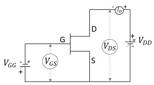
Let us try to summarize the function of FET through which we can obtain the characteristic curve for drain of FET. The circuit of FET to obtain these characteristics is given below.
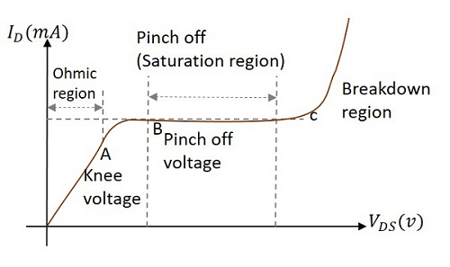
When the voltage between gate and source VGS is zero, or they are shorted, the current ID from source to drain is also nil as there is no VDS applied. As the voltage between drain and source VDS is increased, the current flow ID from source to drain increases. This increase in current is linear up to a certain point A, known as Knee Voltage.
The gate terminals will be under reverse biased condition and as ID increases, the depletion regions tend to constrict. This constriction is unequal in length making these regions come closer at drain and farther at drain, which leads to pinch off voltage. The pinch off voltage is defined as the minimum drain to source voltage where the drain current approaches a constant value (saturation value). The point at which this pinch off voltage occurs is called as Pinch off point, denoted as B.
As VDS is further increased, the channel resistance also increases in such a way that ID practically remains constant. The region BC is known as saturation region or amplifier region. All these along with the points A, B and C are plotted in the graph below.
The drain characteristics are plotted for drain current ID against drain source voltage VDS for different values of gate source voltage VGS. The overall drain characteristics for such various input voltages is as given under.
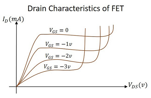
As the negative gate voltage controls the drain current, FET is called as a Voltage controlled device. The drain characteristics indicate the performance of a FET. The drain characteristics plotted above are used to obtain the values of Drain resistance, Transconductance and Amplification Factor.
Basic Electronics - MOSFET
FETs have a few disadvantages like high drain resistance, moderate input impedance and slower operation. To overcome these disadvantages, the MOSFET which is an advanced FET is invented.
MOSFET stands for Metal Oxide Silicon Field Effect Transistor or Metal Oxide Semiconductor Field Effect Transistor. This is also called as IGFET meaning Insulated Gate Field Effect Transistor. The FET is operated in both depletion and enhancement modes of operation. The following figure shows how a practical MOSFET looks like.
Construction of a MOSFET
The construction of a MOSFET is a bit similar to the FET. An oxide layer is deposited on the substrate to which the gate terminal is connected. This oxide layer acts as an insulator (sio2 insulates from the substrate), and hence the MOSFET has another name as IGFET. In the construction of MOSFET, a lightly doped substrate, is diffused with a heavily doped region. Depending upon the substrate used, they are called as P-type and N-type MOSFETs.
The following figure shows the construction of a MOSFET.
The voltage at gate controls the operation of the MOSFET. In this case, both positive and negative voltages can be applied on the gate as it is insulated from the channel. With negative gate bias voltage, it acts as depletion MOSFET while with positive gate bias voltage it acts as an Enhancement MOSFET.
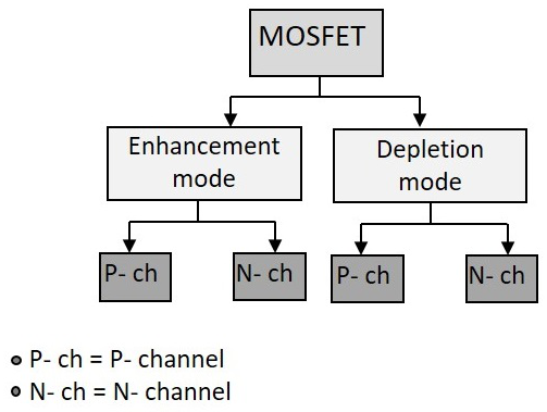
Classification of MOSFETs
Depending upon the type of materials used in the construction, and the type of operation, the MOSFETs are classified as in the following figure.
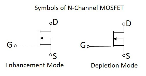
After the classification, let us go through the symbols of MOSFET.
The N-channel MOSFETs are simply called as NMOS. The symbols for N-channel MOSFET are as given below.
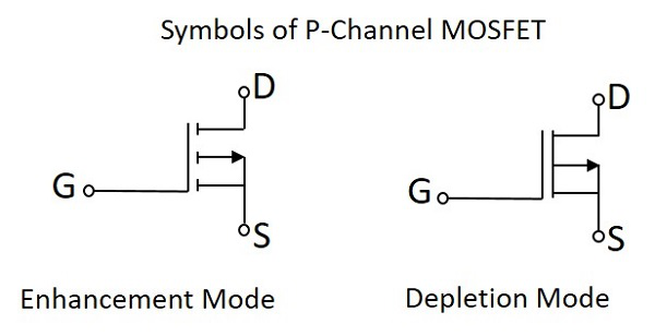
The P-channel MOSFETs are simply called as PMOS. The symbols for P-channel MOSFET are as given below.
Now, let us go through the constructional details of an N-channel MOSFET. Usually an NChannel MOSFET is considered for explanation as this one is mostly used. Also, there is no need to mention that the study of one type explains the other too.
Construction of N- Channel MOSFET
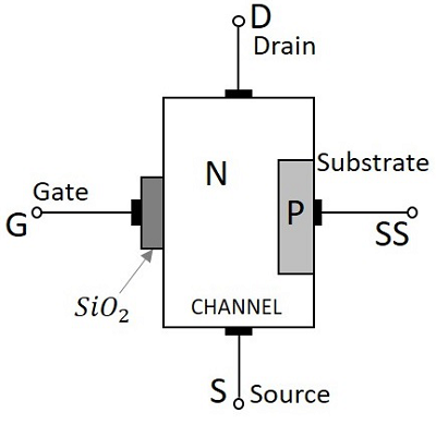
Let us consider an N-channel MOSFET to understand its working. A lightly doped P-type substrate is taken into which two heavily doped N-type regions are diffused, which act as source and drain. Between these two N+ regions, there occurs diffusion to form an Nchannel, connecting drain and source.
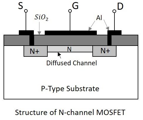
A thin layer of Silicon dioxide (SiO2) is grown over the entire surface and holes are made to draw ohmic contacts for drain and source terminals. A conducting layer of aluminum is laid over the entire channel, upon this SiO2layer from source to drain which constitutes the gate. The SiO2 substrate is connected to the common or ground terminals.
Because of its construction, the MOSFET has a very less chip area than BJT, which is 5% of the occupancy when compared to bipolar junction transistor. This device can be operated in modes. They are depletion and enhancement modes. Let us try to get into the details.
Working of N - Channel (depletion mode) MOSFET
For now, we have an idea that there is no PN junction present between gate and channel in this, unlike a FET. We can also observe that, the diffused channel N (between two N+ regions), the insulating dielectric SiO2 and the aluminum metal layer of the gate together form a parallel plate capacitor.
If the NMOS has to be worked in depletion mode, the gate terminal should be at negative potential while drain is at positive potential, as shown in the following figure.
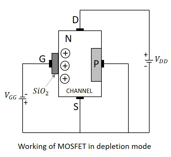
When no voltage is applied between gate and source, some current flows due to the voltage between drain and source. Let some negative voltage is applied at VGG. Then the minority carriers i.e. holes, get attracted and settle near SiO2layer. But the majority carriers, i.e., electrons get repelled.
With some amount of negative potential at VGG a certain amount of drain current ID flows through source to drain. When this negative potential is further increased, the electrons get depleted and the current ID decreases. Hence the more negative the applied VGG, the lesser the value of drain current ID will be.
The channel nearer to drain gets more depleted than at source (like in FET) and the current flow decreases due to this effect. Hence it is called as depletion mode MOSFET.


