


Common Emitter (CE) Configuration
The name itself implies that the Emitter terminal is taken as common terminal for both input and output of the transistor. The common emitter connection for both NPN and PNP transistors is as shown in the following figure.
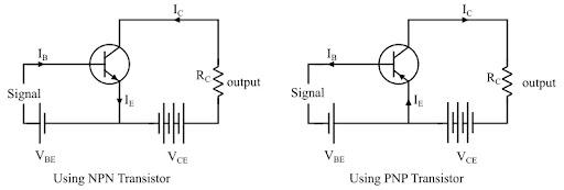
Just as in CB configuration, the emitter junction is forward biased and the collector junction is reverse biased. The flow of electrons is controlled in the same manner. The input current is the base current IB and the output current is the collector current IC here.
Base Current Amplification factor (β)
The ratio of change in collector current () to the change in base current () is known as Base Current Amplification Factor. It is denoted by β
Relation between β and α
Let us try to derive the relation between base current amplification factor and emitter current amplification factor.
We can write
Dividing by $$
We have
Therefore,
From the above equation, it is evident that, as α approaches 1, β reaches infinity.
Hence, the current gain in Common Emitter connection is very high. This is the reason this circuit connection is mostly used in all transistor applications.
Expression for Collector Current
In the Common Emitter configuration, IB is the input current and IC is the output current.
We know
And
If base circuit is open, i.e. if IB = 0,
The collector emitter current with base open is ICEO
Substituting the value of this in the previous equation, we get
Hence the equation for collector current is obtained.
Knee Voltage
In CE configuration, by keeping the base current IB constant, if VCE is varied, ICincreases nearly to 1v of VCE and stays constant thereafter. This value of VCEup to which collector current IC changes with VCE is called the Knee Voltage. The transistors while operating in CE configuration, they are operated above this knee voltage.
Characteristics of CE Configuration
- This configuration provides good current gain and voltage gain.
- Keeping VCE constant, with a small increase in VBE the base current IBincreases rapidly than in CB configurations.
- For any value of VCE above knee voltage, IC is approximately equal to βIB.
- The input resistance ri is the ratio of change in base emitter voltage () to the change in base current () at constant collector emitter voltage VCE.
- As the input resistance is of very low value, a small value of VBE is enough to produce a large current flow of base current IB.
- The output resistance ro is the ratio of change in collector emitter voltage () to the change in collector current () at constant IB.
- As the output resistance of CE circuit is less than that of CB circuit.
- This configuration is usually used for bias stabilization methods and audio frequency applications.
Common Collector (CC) Configuration
The name itself implies that the Collector terminal is taken as common terminal for both input and output of the transistor. The common collector connection for both NPN and PNP transistors is as shown in the following figure.
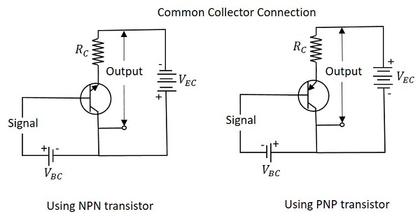
Just as in CB and CE configurations, the emitter junction is forward biased and the collector junction is reverse biased. The flow of electrons is controlled in the same manner. The input current is the base current IB and the output current is the emitter current IE here.
Current Amplification Factor (γ)
The ratio of change in emitter current () to the change in base current () is known as Current Amplification factor in common collector (CC) configuration. It is denoted by γ.
- The current gain in CC configuration is same as in CE configuration.
- The voltage gain in CC configuration is always less than 1.
Relation between γ and α
Let us try to draw some relation between γ and α
Substituting the value of IB, we get
Dividing by
Expression for collector current
We know
The above is the expression for collector current.
Characteristics of CC Configuration
- This configuration provides current gain but no voltage gain.
- In CC configuration, the input resistance is high and the output resistance is low.
- The voltage gain provided by this circuit is less than 1.
- The sum of collector current and base current equals emitter current.
- The input and output signals are in phase.
- This configuration works as non-inverting amplifier output.
- This circuit is mostly used for impedance matching. That means, to drive a low impedance load from a high impedance source.
Transistor Regions of Operation
The DC supply is provided for the operation of a transistor. This DC supply is given to the two PN junctions of a transistor which influences the actions of majority carriers in these emitter and collector junctions.
The junctions are forward biased and reverse biased based on our requirement. Forward biased is the condition where a positive voltage is applied to the p-type and negative voltage is applied to the n-type material. Reverse biased is the condition where a positive voltage is applied to the n-type and negative voltage is applied to the p-type material.
Transistor biasing
The supply of suitable external dc voltage is called as biasing. Either forward or reverse biasing is done to the emitter and collector junctions of the transistor. These biasing methods make the transistor circuit to work in four kinds of regions such as Active region, Saturation region, Cutoff region and Inverse active region (seldom used). This is understood by having a look at the following table.
| EMITTER JUNCTION | COLLECTOR JUNCTION | REGION OF OPERATION |
|---|---|---|
| Forward biased | Forward biased | Saturation region |
| Forward biased | Reverse biased | Active region |
| Reverse biased | Forward biased | Inverse active region |
| Reverse biased | Reverse biased | Cutoff region |
Among these regions, Inverse active region, which is just the inverse of active region, is not suitable for any applications and hence not used.
Active region
This is the region in which transistors have many applications. This is also called as linear region. A transistor while in this region, acts better as an Amplifier.
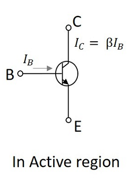
This region lies between saturation and cutoff. The transistor operates in active region when the emitter junction is forward biased and collector junction is reverse biased. In the active state, collector current is β times the base current, i.e.,
Where,
= collector current
= current amplification factor
= base current
Saturation region
This is the region in which transistor tends to behave as a closed switch. The transistor has the effect of its collector and Emitter being shorted. The collector and Emitter currents are maximum in this mode of operation.
The figure below shows a transistor working in saturation region.
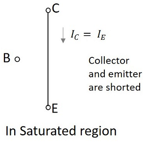
The transistor operates in saturation region when both the emitter and collector junctions are forward biased. As it is understood that, in the saturation region the transistor tends to behave as a closed switch, we can say that,
Where = collector current and = emitter current.
Cutoff region
This is the region in which transistor tends to behave as an open switch. The transistor has the effect of its collector and base being opened. The collector, emitter and base currents are all zero in this mode of operation.
The following figure shows a transistor working in cutoff region.
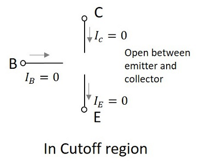
The transistor operates in cutoff region when both the emitter and collector junctions are reverse biased. As in cutoff region, the collector current, emitter current and base currents are nil, we can write as
Where = collector current, = emitter current, and = base current.
Transistor Load Line Analysis
Till now we have discussed different regions of operation for a transistor. But among all these regions, we have found that the transistor operates well in active region and hence it is also called as linear region. The outputs of the transistor are the collector current and collector voltages.
Output Characteristics
When the output characteristics of a transistor are considered, the curve looks as below for different input values.
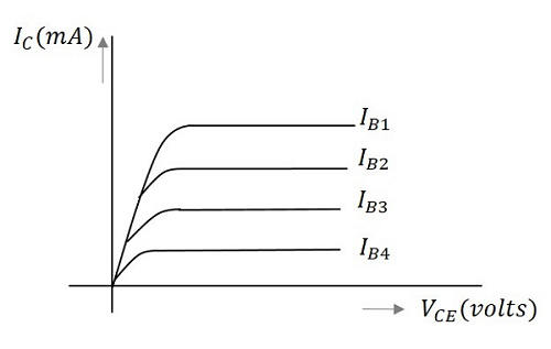
In the above figure, the output characteristics are drawn between collector current IC and collector voltage VCE for different values of base current IB. These are considered here for different input values to obtain different output curves.
Operating point
When a value for the maximum possible collector current is considered, that point will be present on the Y-axis, which is nothing but the saturation point. As well, when a value for the maximum possible collector emitter voltage is considered, that point will be present on the X-axis, which is the cutoff point.
When a line is drawn joining these two points, such a line can be called as Load line. This is called so as it symbolizes the output at the load. This line, when drawn over the output characteristic curve, makes contact at a point called as Operating point.
This operating point is also called as quiescent point or simply Q-point. There can be many such intersecting points, but the Q-point is selected in such a way that irrespective of AC signal swing, the transistor remains in active region. This can be better understood through the figure below.
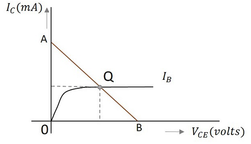
The load line has to be drawn in order to obtain the Q-point. A transistor acts as a good amplifier when it is in active region and when it is made to operate at Q-point, faithful amplification is achieved.
Faithful amplification is the process of obtaining complete portions of input signal by increasing the signal strength. This is done when AC signal is applied at its input. This is discussed in AMPLIFIERS tutorial.
DC Load line
When the transistor is given the bias and no signal is applied at its input, the load line drawn at such condition, can be understood as DC condition. Here there will be no amplification as the signal is absent. The circuit will be as shown below.
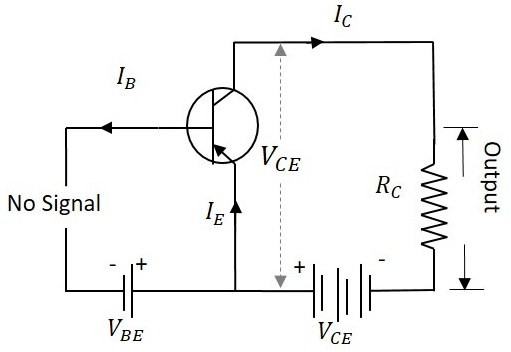
The value of collector emitter voltage at any given time will be
As VCC and RC are fixed values, the above one is a first degree equation and hence will be a straight line on the output characteristics. This line is called as D.C. Load line. The figure below shows the DC load line.
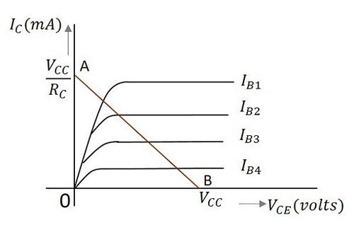
To obtain the load line, the two end points of the straight line are to be determined. Let those two points be A and B.
To obtain A
When collector emitter voltage VCE = 0, the collector current is maximum and is equal to VCC/RC. This gives the maximum value of VCE. This is shown as
This gives the point A (OA = VCC/RC) on collector current axis, shown in the above figure.
To obtain B
When the collector current IC = 0, then collector emitter voltage is maximum and will be equal to the VCC. This gives the maximum value of IC. This is shown as
(As IC = 0)
This gives the point B, which means (OB = VCC) on the collector emitter voltage axis shown in the above figure.
Hence we got both the saturation and cutoff point determined and learnt that the load line is a straight line. So, a DC load line can be drawn.
The importance of this operating point is further understood when an AC signal is given at the input. This will be discussed in AMPLIFIERS tutorial.


