


Basic Electronics - Transistors
After having a good knowledge on the working of the diode, which is a single PN junction, let us try to connect two PN junctions which make a new component called Transistor. A Transistor is a three terminal semiconductor device that regulates current or voltage flow and acts as a switch or gate for signals.
Why Do We Need Transistors?
Suppose that you have a FM receiver which grabs the signal you want. The received signal will obviously be weak due to the disturbances it would face during its journey. Now if this signal is read as it is, you cannot get a fair output. Hence we need to amplify the signal. Amplification means increasing the signal strength.
This is just an instance. Amplification is needed wherever the signal strength has to be increased. This is done by a transistor. A transistor also acts as a switch to choose between available options. It also regulates the incoming current and voltage of the signals.
Constructional Details of a Transistor
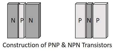
The Transistor is a three terminal solid state device which is formed by connecting two diodes back to back. Hence it has got two PN junctions. Three terminals are drawn out of the three semiconductor materials present in it. This type of connection offers two types of transistors. They are PNP and NPN which means an N-type material between two Ptypes and the other is a P-type material between two N-types respectively.
The construction of transistors is as shown in the following figure which explains the idea discussed above.
The three terminals drawn from the transistor indicate Emitter, Base and Collector terminals. They have their functionality as discussed below.
Emitter
- The left hand side of the above shown structure can be understood as Emitter.
- This has a moderate size and is heavily doped as its main function is to supply a number of majority carriers, i.e. either electrons or holes.
- As this emits electrons, it is called as an Emitter.
- This is simply indicated with the letter E.
Base
- The middle material in the above figure is the Base.
- This is thin and lightly doped.
- Its main function is to pass the majority carriers from the emitter to the collector.
- This is indicated by the letter B.
Collector
- The right side material in the above figure can be understood as a Collector.
- Its name implies its function of collecting the carriers.
- This is a bit larger in size than emitter and base. It is moderately doped.
- This is indicated by the letter C.
The symbols of PNP and NPN transistors are as shown below.
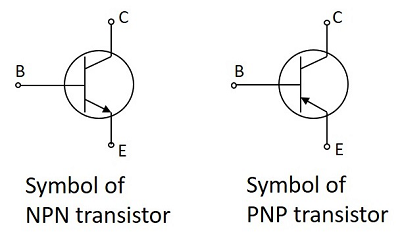
The arrow-head in the above figures indicated the emitter of a transistor. As the collector of a transistor has to dissipate much greater power, it is made large. Due to the specific functions of emitter and collector, they are not interchangeable. Hence the terminals are always to be kept in mind while using a transistor.
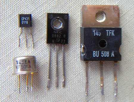
In a Practical transistor, there is a notch present near the emitter lead for identification. The PNP and NPN transistors can be differentiated using a Multimeter. The following figure shows how different practical transistors look like.
We have so far discussed the constructional details of a transistor, but to understand the operation of a transistor, first we need to know about the biasing.
Transistor Biasing
As we know that a transistor is a combination of two diodes, we have two junctions here. As one junction is between the emitter and base, that is called as Emitter-Base junction and likewise, the other is Collector-Base junction.
Biasing is controlling the operation of the circuit by providing power supply. The function of both the PN junctions is controlled by providing bias to the circuit through some dc supply. The figure below shows how a transistor is biased.
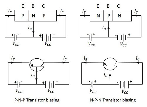
By having a look at the above figure, it is understood that
- The N-type material is provided negative supply and P-type material is given positive supply to make the circuit Forward bias.
- The N-type material is provided positive supply and P-type material is given negative supply to make the circuit Reverse bias.
By applying the power, the emitter base junction is always forward biased as the emitter resistance is very small. The collector base junction is reverse biased and its resistance is a bit higher. A small forward bias is sufficient at the emitter junction whereas a high reverse bias has to be applied at the collector junction.
The direction of current indicated in the circuits above, also called as the Conventional Current, is the movement of hole current which is opposite to the electron current.
Operation PNP Transistor
The operation of a PNP transistor can be explained by having a look at the following figure, in which emitter-base junction is forward biased and collector-base junction is reverse biased.
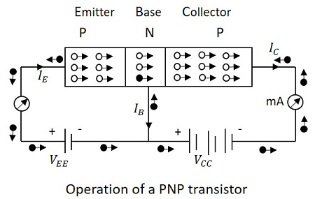
The voltage VEE provides a positive potential at the emitter which repels the holes in the P-type material and these holes cross the emitter-base junction, to reach the base region. There a very low percent of holes recombine with free electrons of N-region. This provides very low current which constitutes the base current IB. The remaining holes cross the collector-base junction, to constitute collector current IC, which is the hole current.
As a hole reaches the collector terminal, an electron from the battery negative terminal fills the space in the collector. This flow slowly increases and the electron minority current flows through the emitter, where each electron entering the positive terminal of VEE, is replaced by a hole by moving towards the emitter junction. This constitutes emitter current IE.
Hence we can understand that −
- The conduction in a PNP transistor takes place through holes.
- The collector current is slightly less than the emitter current.
- The increase or decrease in the emitter current affects the collector current.
Operation NPN Transistor
The operation of an NPN transistor can be explained by having a look at the following figure, in which emitter-base junction is forward biased and collector-base junction is reverse biased.
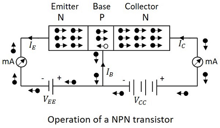
The voltage VEE provides a negative potential at the emitter which repels the electrons in the N-type material and these electrons cross the emitter-base junction, to reach the base region. There a very low percent of electrons recombine with free holes of P-region. This provides very low current which constitutes the base current IB. The remaining holes cross the collector-base junction, to constitute the collector current IC.
As an electron reaches out of the collector terminal, and enters the positive terminal of the battery, an electron from the negative terminal of the battery VEE enters the emitter region. This flow slowly increases and the electron current flows through the transistor.
Hence we can understand that −
- The conduction in a NPN transistor takes place through electrons.
- The collector current is higher than the emitter current.
- The increase or decrease in the emitter current affects the collector current.
Advantages
There are many advantages of a transistor such as −
- High voltage gain.
- Lower supply voltage is sufficient.
- Most suitable for low power applications.
- Smaller and lighter in weight.
- Mechanically stronger than vacuum tubes.
- No external heating required like vacuum tubes.
- Very suitable to integrate with resistors and diodes to produce ICs.
There are few disadvantages such as they cannot be used for high power applications due to lower power dissipation. They have lower input impedance and they are temperature dependent.
Basic Electronics - Transistor Configurations
A Transistor has 3 terminals, the emitter, the base and the collector. Using these 3 terminals the transistor can be connected in a circuit with one terminal common to both input and output in a 3 different possible configurations.
The three types of configurations are Common Base, Common Emitter and Common Collector configurations. In every configuration, the emitter junction is forward biased and the collector junction is reverse biased.
Common Base (CB) Configuration
The name itself implies that the Base terminal is taken as common terminal for both input and output of the transistor. The common base connection for both NPN and PNP transistors is as shown in the following figure.
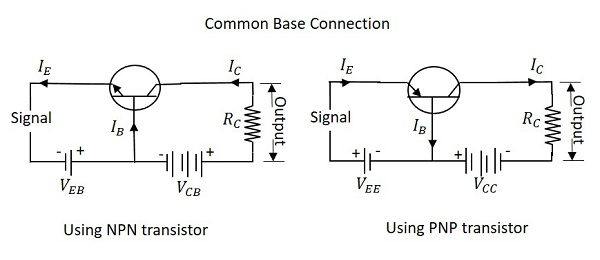
For the sake of understanding, let us consider NPN transistor in CB configuration. When the emitter voltage is applied, as it is forward biased, the electrons from the negative terminal repel the emitter electrons and current flows through the emitter and base to the collector to contribute collector current. The collector voltage VCB is kept constant throughout this.
In the CB configuration, the input current is the emitter current IE and the output current is the collector current IC.
Current Amplification Factor (α)
The ratio of change in collector current () to the change in emitter current () when collector voltage VCB is kept constant, is called as Current amplification factor. It is denoted by α.
Expression for Collector current
With the idea above, let us try to draw some expression for collector current. Along with the emitter current flowing, there is some amount of base current IB which flows through the base terminal due to electron hole recombination. As collector-base junction is reverse biased, there is another current which is flown due to minority charge carriers. This is the leakage current which can be understood as Ileakage. This is due to minority charge carriers and hence very small.
The emitter current that reaches the collector terminal is
Total collector current
If the emitter-base voltage VEB = 0, even then, there flows a small leakage current, which can be termed as ICBO (collector-base current with output open).
The collector current therefore can be expressed as
Hence the above derived is the expression for collector current. The value of collector current depends on base current and leakage current along with the current amplification factor of that transistor in use.
Characteristics of CB configuration
- This configuration provides voltage gain but no current gain.
- Being VCB constant, with a small increase in the Emitter-base voltage VEB, Emitter current IE gets increased.
- Emitter Current IE is independent of Collector voltage VCB.
- Collector Voltage VCB can affect the collector current IC only at low voltages, when VEB is kept constant.
- The input resistance ri is the ratio of change in emitter-base voltage () to the change in emitter current () at constant collector base voltage VCB.
- As the input resistance is of very low value, a small value of VEB is enough to produce a large current flow of emitter current IE.
- The output resistance ro is the ratio of change in the collector base voltage () to the change in collector current () at constant emitter current IE.
- As the output resistance is of very high value, a large change in VCBproduces a very little change in collector current IC.
- This Configuration provides good stability against increase in temperature.
- The CB configuration is used for high frequency applications.


