


Working of N-Channel MOSFET (Enhancement Mode)
The same MOSFET can be worked in enhancement mode, if we can change the polarities of the voltage VGG. So, let us consider the MOSFET with gate source voltage VGG being positive as shown in the following figure.
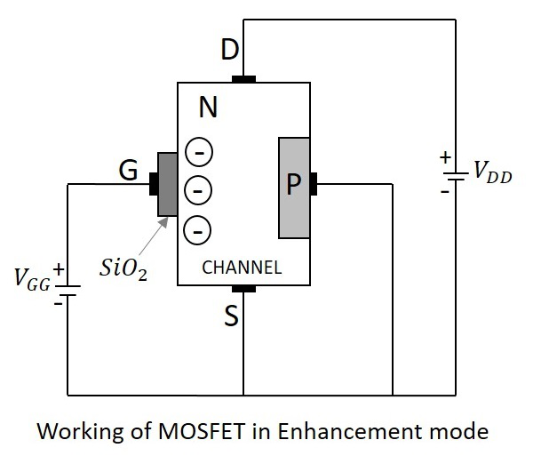
When no voltage is applied between gate and source, some current flows due to the voltage between drain and source. Let some positive voltage is applied at VGG. Then the minority carriers i.e. holes, get repelled and the majority carriers i.e. electrons gets attracted towards the SiO2 layer.
With some amount of positive potential at VGG a certain amount of drain current ID flows through source to drain. When this positive potential is further increased, the current ID increases due to the flow of electrons from source and these are pushed further due to the voltage applied at VGG. Hence the more positive the applied VGG, the more the value of drain current ID will be. The current flow gets enhanced due to the increase in electron flow better than in depletion mode. Hence this mode is termed as Enhanced Mode MOSFET.
P - Channel MOSFET
The construction and working of a PMOS is same as NMOS. A lightly doped n-substrate is taken into which two heavily doped P+ regions are diffused. These two P+ regions act as source and drain. A thin layer of SiO2 is grown over the surface. Holes are cut through this layer to make contacts with P+ regions, as shown in the following figure.
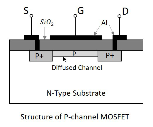
Working of PMOS
When the gate terminal is given a negative potential at VGG than the drain source voltage VDD, then due to the P+ regions present, the hole current is increased through the diffused P channel and the PMOS works in Enhancement Mode.
When the gate terminal is given a positive potential at VGG than the drain source voltage VDD, then due to the repulsion, the depletion occurs due to which the flow of current reduces. Thus PMOS works in Depletion Mode. Though the construction differs, the working is similar in both the type of MOSFETs. Hence with the change in voltage polarity both of the types can be used in both the modes.
This can be better understood by having an idea on the drain characteristics curve.
Drain Characteristics
The drain characteristics of a MOSFET are drawn between the drain current IDand the drain source voltage VDS. The characteristic curve is as shown below for different values of inputs.
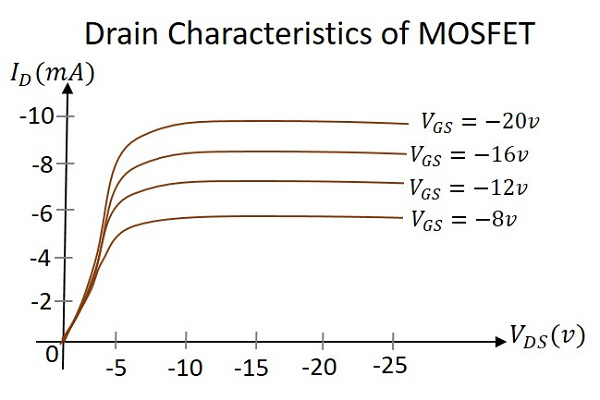
Actually when VDS is increased, the drain current ID should increase, but due to the applied VGS, the drain current is controlled at certain level. Hence the gate current controls the output drain current.
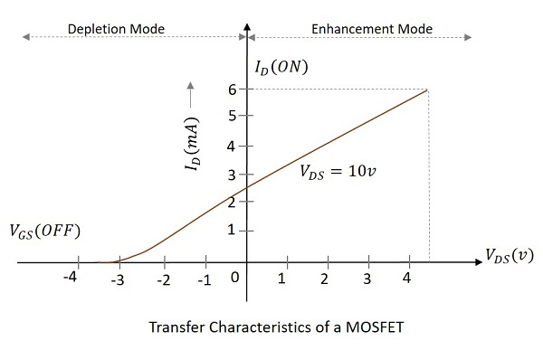
Transfer Characteristics
Transfer characteristics define the change in the value of VDS with the change in ID and VGS in both depletion and enhancement modes. The below transfer characteristic curve is drawn for drain current versus gate to source voltage.
Comparison between BJT, FET and MOSFET
Now that we have discussed all the above three, let us try to compare some of their properties.
| TERMS | BJT | FET | MOSFET |
|---|---|---|---|
| Device type | Current controlled | Voltage controlled | Voltage Controlled |
| Current flow | Bipolar | Unipolar | Unipolar |
| Terminals | Not interchangeable | Interchangeable | Interchangeable |
| Operational modes | No modes | Depletion mode only | Both Enhancement and Depletion modes |
| Input impedance | Low | High | Very high |
| Output resistance | Moderate | Moderate | Low |
| Operational speed | Low | Moderate | High |
| Noise | High | Low | Low |
| Thermal stability | Low | Better | High |
So far, we have discussed various electronic components and their types along with their construction and working. All of these components have various uses in the electronics field. To have a practical knowledge on how these components are used in practical circuits, please refer to the ELECTRONIC CIRCUITS tutorial.


