


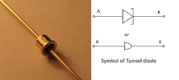
unnel diode
If the impurity concentration of a normal PN junction is highly increased, this Tunnel diode is formed. It is also known as Esaki diode, after its inventor.
When the impurity concentration in a diode increases, the width of depletion region decreases, extending some extra force to the charge carriers to cross the junction. When this concentration is further increased, due to less width of the depletion region and the increased energy of the charge carriers, they penetrate through the potential barrier, instead of climbing over it. This penetration can be understood as Tunneling and hence the name, Tunnel diode.
The Tunnel diodes are low power devices and should be handled with care as they easily get affected by heat and static electricity. The Tunnel diode has specific V-I characteristics which explain their working. Let us have a look at the graph below.
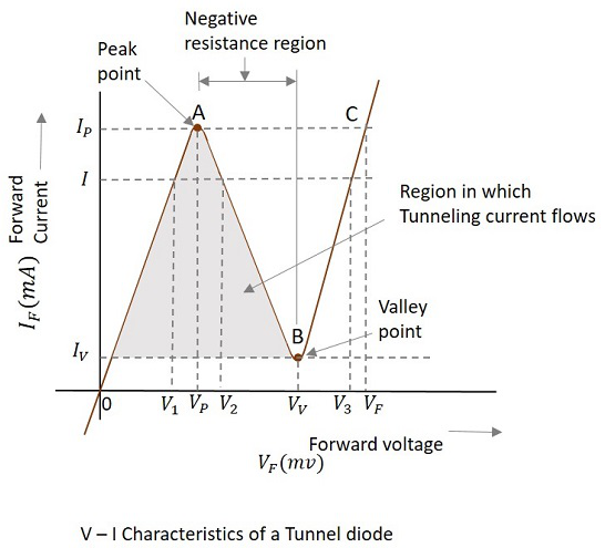
Consider the diode is in forward-biased condition. As forward voltage increases, the current increases rapidly and it increases until a peak point, called as Peak Current, denoted by IP. The voltage at this point is called as Peak Voltage, denoted by VP. This point is indicated by A in the above graph.
If the voltage is further increased beyond VP, then the current starts decreasing. It decreases until a point, called as Valley Current, denoted by IV. The voltage at this point is called as Valley Voltage, denoted by VV. This point is indicated by B in the above graph.
If the voltage is increased further, the current increases as in a normal diode. For larger values of forward voltage, the current increases further beyond.
If we consider the diode is in reverse-biased condition, then the diode acts as an excellent conductor as the reverse voltage increases. The diode here acts as in a negative resistance region.
Applications of Tunnel diode
There are many applications for tunnel diode such as −
- Used as a high-Speed Switching device
- Used as a memory storage device
- Used in Microwave oscillators
- Used in relaxation oscillators
Schottky Diode
This is a special type of diode in which a PN junction is replaced by a metal semiconductor junction. The P-type semiconductor in a normal PN junction diode is replaced by a metal and N-type material is joined to the metal. This combination has no depletion region between them. The following figure shows the Schottky diode and its symbol.
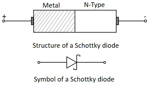
The metal used in this Schottky diode may be gold, silver, platinum or tungsten etc. As well, for the semiconductor material other than silicon, gallium arsenide is mostly used.
Operation
When no voltage is applied or when the circuit is unbiased, the electrons in the N-type material has lower energy level than the ones in the metal. If the diode is then forward biased, these electrons in the N-type gain some energy and move with some higher energy. Hence these electrons are called as Hot Carriers.
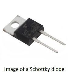
The following figure shows a Schottky diode connected in a circuit.
Advantages
There are many advantages of Schottky diode such as −
- It is a unipolar device and hence no reverse currents are formed.
- Its forward resistance is low.
- Voltage drops are very low.
- Rectification is fast and easy with the Schottky diode.
- There is no depletion region present and hence, no junction capacitance. So, the diode gets to OFF position quickly.
Applications
There are many applications of Schottky diode such as −
- Used as a detector diode
- Used as a Power rectifier
- Used in RF mixer circuits
- Used in power circuits
- Used as clamping diodes
Basic Electronics - Optoelectronic Diodes
These are the diodes which are operated on light. The word “Opto” means Light. There are types that conduction depending upon the light intensity and other types whose conduction delivers some light. Each type has got applications of their own. Let us discuss the prominent types among these ones.
Some diodes conduct according to the intensity of light falls on them. There are two main types of diodes in this category. They are Photo diodes and Solar cells.
Photo Diode
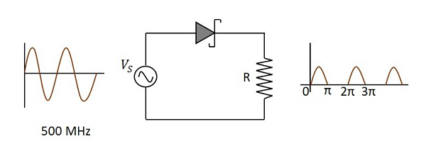
Photo diode, as the name implies, is a PN junction which works on light. The intensity of light affects the level of conduction in this diode. The photo diode has a P type material and an N-type material with an intrinsic material or a depletion region in between.
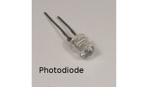
This diode is generally operated in reverse bias condition. The light when focused on the depletion region, electron-hole pairs are formed and flow of electron occurs. This conduction of electrons depends upon the intensity of light focused. The figure below shows a practical Photo diode.
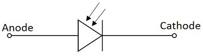
The figure below indicates the symbol for a photodiode.
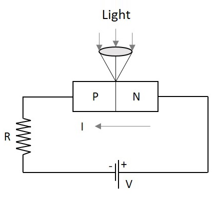
When the diode is connected in reverse bias, a small reverse saturation current flows due to thermally generated electron hole pairs. As the current in reverse bias flows due to minority carriers, the output voltage depends upon this reverse current. As the light intensity focused on the junction increases, the current flow due to minority carriers increase. The following figure shows the basic biasing arrangement of a photo diode.
The Photo diode is encapsulated in a glass package to allow the light to fall onto it. In order to focus the light exactly on the depletion region of the diode, a lens is placed above the junction, just as illustrated above.
Even when there is no light, a small amount of current flows which is termed as Dark Current. By changing the illumination level, reverse current can be changed.
Advantages of Photo diode
Photo diode has many advantages such as −
- Low noise
- High gain
- High speed operation
- High sensitivity to light
- Low cost
- Small size
- Long lifetime
Applications of Photo diode
There are many applications for photo diode such as −
- Character detection
- Objects can be detected (visible or invisible).
- Used in circuits that require high stability and speed.
- Used in Demodulation
- Used in switching circuits
- Used in Encoders
- Used in optical communication equipment
Another diode of such a kind is Solar cell. It is termed as a cell though it is a diode. Let us get into the details.
Solar Cell
The light dependent diodes include Solar cell, which is a normal PN junction diode but has its conduction by the rush of photons which are converted into the flow of electrons. This is similar to a photo diode but it has another objective of converting maximum incident light into energy and storing it.
The figure below represents the symbol of a solar cell.
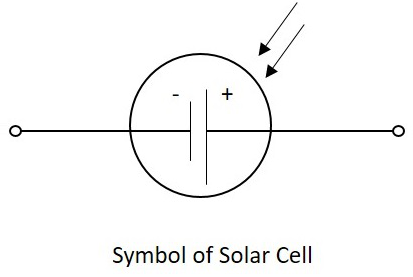
A solar cell has its name and symbol indicating storing of energy though it is a diode. The feature of extracting more energy and storing of it is concentrated in the solar cell.
Construction of a Solar cell
A PN junction diode with an intrinsic material in the deletion region is made to encapsulate in a glass. The light is made to incident on maximum area possible with thin glass on the top so as to collect maximum light with minimum resistance.
The following figure shows the construction of a Solar cell.
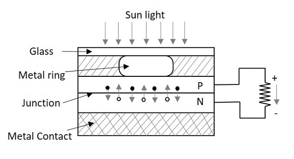
When the light is incident on the solar cell, the photons in the light collide with valence electrons. The electrons are energized to leave the parent atoms. Thus a flow of electrons is generated and this current is directly proportional to the light intensity focused onto the solar cell. This phenomenon is called as the Photo-Voltaic effect.
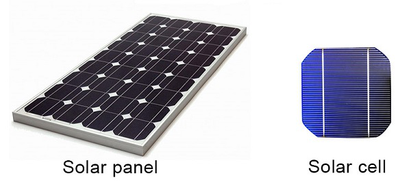
The following figure shows how a solar cell looks like and how a number of solar cells together are made to form a solar panel.
Difference between a Photo diode and Solar cell
Photo Diode works faster and concentrates on switching rather than providing more power at the output. It has a low capacitance value because of this. Also the area of incidence of light energy is lesser in Photo diode, according to its applications.
A Solar cell concentrates on delivering high output energy and storing the energy. This has high capacitance value. The operation is a bit slower than photo diode. According to the purpose of the solar cell, the area of incidence of light is larger than photo diode.
Applications of Solar Cell
There are many applications for Solar cell such as −
Science and Technology
- Used in Solar panels for Satellites
- Used in telemetry
- Used in Remote lighting systems etc.
Commercial Use
- Used in Solar panels for storage of electricity
- Used in Portable power supplies etc.
- Used in household uses such as cooking and heating using solar energy
Electronic
- Watches
- Calculators
- Electronic Toys, etc.
Some diodes emit light according to the voltage applied. There are two main types of diodes in this category. They are LEDs and Laser diodes.


