


DC Load line
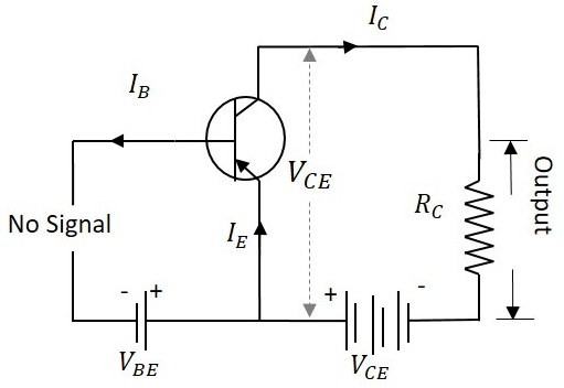
When the transistor is given the bias and no signal is applied at its input, the load line drawn at such condition, can be understood as DC condition. Here there will be no amplification as the signal is absent. The circuit will be as shown below.
The value of collector emitter voltage at any given time will be
As VCC and RC are fixed values, the above one is a first degree equation and hence will be a straight line on the output characteristics. This line is called as D.C. Load line. The figure below shows the DC load line.
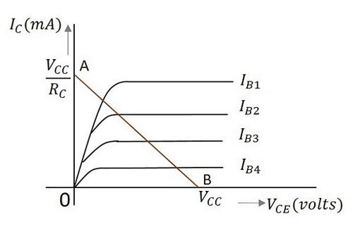
To obtain the load line, the two end points of the straight line are to be determined. Let those two points be A and B.
To obtain A
When collector emitter voltage VCE = 0, the collector current is maximum and is equal to VCC/RC. This gives the maximum value of VCE. This is shown as
This gives the point A (OA = VCC/RC) on collector current axis, shown in the above figure.
To obtain B
When the collector current IC = 0, then collector emitter voltage is maximum and will be equal to the VCC. This gives the maximum value of IC. This is shown as
(As IC = 0)
This gives the point B, which means (OB = VCC) on the collector emitter voltage axis shown in the above figure.
Hence we got both the saturation and cutoff point determined and learnt that the load line is a straight line. So, a DC load line can be drawn.
The importance of this operating point is further understood when an AC signal is given at the input. This will be discussed in AMPLIFIERS tutorial.
Basic Electronics - Types of Transistors
There are many types of transistors in use. Each transistor is specialized in its application. The main classification is as follows.
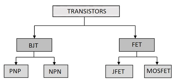
The primary transistor is the BJT and FET is the modern version of transistor. Let us have a look at the BJTs.
Bipolar Junction Transistor
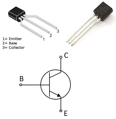
A Bipolar junction transistor, shortly termed as BJT is called so as it has two PN junctions for its function. This BJT is nothing but a normal transistor. It has got two types of configurations NPN and PNP. Usually NPN transistor is preferred for the sake of convenience. The following image shows how a practical BJT looks like.
The types of BJT are NPN and PNP transistors. The NPN transistor is made by placing a ptype material between two n-type materials. The PNP transistor is made by placing an ntype material between two p-type materials.
BJT is a current controlled device. A normal transistor which we had discussed in the previous chapters come under this category. The functionality, configurations and applications are all the same.
Field Effect Transistor
An FET is a three-terminal unipolar semiconductor device. It is a voltage controlled device unlike a bipolar junction transistor. The main advantage of FET is that it has a very high input impedance, which is in the order of Mega Ohms. It has many advantages like low power consumption, low heat dissipation and FETs are highly efficient devices. The following image shows how a practical FET looks like.
The FET is a unipolar device, which means that it is made using either p-type or n-type material as main substrate. Hence the current conduction of a FET is done by either electrons or holes.
Features of FET
The following are the varied features of a Field Effect Transistor.
- Unipolar − It is unipolar as either holes or electrons are responsible for conduction.
- High input impedance − The input current in a FET flows due to the reverse bias. Hence it has high input impedance.
- Voltage controlled device − As the output voltage of a FET is controlled by the gate input voltage, FET is called as the voltage controlled device.
- Noise is low − There are no junctions present in the conduction path. Hence noise is lower than in BJTs.
- Gain is characterized as transconductance. Transconductance is the ratio of change in output current to the change in input voltage.
- The output impedance of a FET is low.
Advantages of FET
To prefer a FET over BJT, there should be few advantages of using FETs, rather than BJTs. Let us try to summarize the advantages of FET over BJT.
| JFET | BJT |
|---|---|
| It is an unipolar device | It is a bipolar device |
| Voltage driven device | Current driven device |
| High input impedance | Low input impedance |
| Low noise level | High noise level |
| Better thermal stability | Less thermal stability |
| Gain is characterized by transconductance | Gain is characterized by voltage gain |
Applications of FET
- FET is used in circuits to reduce the loading effect.
- FETs are used in many circuits such as Buffer Amplifier, Phase shift Oscillators and Voltmeters.
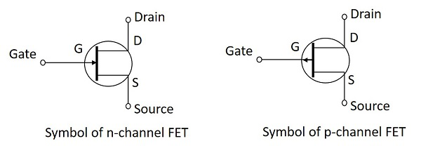
FET Terminals
Though FET is a three terminal device, they are not the same as BJT terminals. The three terminals of FET are Gate, Source and Drain. The Source terminal in FET is analogous to the Emitter in BJT, while Gate is analogous to Base and Drain to Collector.
The symbols of a FET for both NPN and PNP types are as shown below
Source
- The Source terminal in a Field Effect Transistor is the one through which the carriers enter the channel.
- This is analogous to the emitter terminal in a Bipolar Junction Transistor.
- The Source terminal can be designated as S.
- The current entering the channel at Source terminal is indicated as IS.
Gate
- The Gate terminal in a Field Effect Transistor plays a key role in the function of FET by controlling the current through the channel.
- By applying an external voltage at Gate terminal, the current through it can be controlled.
- Gate is a combination of two terminals connected internally that are heavily doped.
- The channel conductivity is said to be modulated by the Gate terminal.
- This is analogous to the base terminal in a Bipolar Junction Transistor.
- The Gate terminal can be designated as G.
- The current entering the channel at Gate terminal is indicated as IG.
Drain
- The Drain terminal in a Field Effect Transistor is the one through which the carriers leave the channel.
- This is analogous to the collector terminal in a Bipolar Junction Transistor.
- The Drain to Source voltage is designated as VDS.
- The Drain terminal can be designated as D.
- The current leaving the channel at Drain terminal is indicated as ID.
Types of FET
There are two main types of FETS. They are JFET and MOSFET. The following figure gives further classification of FETs.
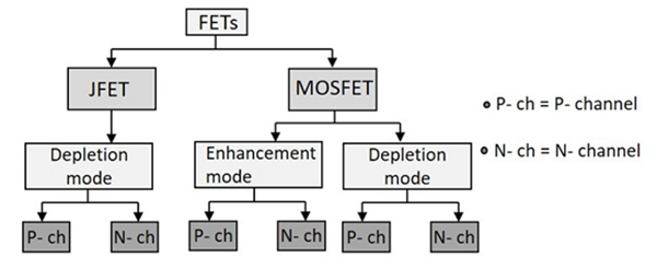
In the subsequent chapters, we will have a detailed discussion on JFET and MOSFET.


