Welcome To SUNTEC Tutorial Point - www.sunteccampus.com

  • SUNTEC

    SUNTEC Computer college

  • Computer Programming

    Computer Programming

  • Web Development

    Web Development

  • Computer Accounting

    Computer Accounting

  • SUNTEC Graphic Designing

    Graphic designing

Working of N-Channel MOSFET (Enhancement Mode)

Working of N-Channel MOSFET (Enhancement Mode)

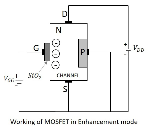
The same MOSFET can be worked in enhancement mode, if we can change the polarities of the voltage VGG. So, let us consider the MOSFET with gate source voltage VGG being positive as shown in the following figure.
N-Channel MOSFET Enhancement
When no voltage is applied between gate and source, some current flows due to the voltage between drain and source. Let some positive voltage is applied at VGG. Then the minority carriers i.e. holes, get repelled and the majority carriers i.e. electrons gets attracted towards the SiO2 layer.
With some amount of positive potential at VGG a certain amount of drain current ID flows through source to drain. When this positive potential is further increased, the current ID increases due to the flow of electrons from source and these are pushed further due to the voltage applied at VGG. Hence the more positive the applied VGG, the more the value of drain current ID will be. The current flow gets enhanced due to the increase in electron flow better than in depletion mode. Hence this mode is termed as Enhanced Mode MOSFET.

P - Channel MOSFET

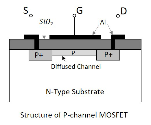
The construction and working of a PMOS is same as NMOS. A lightly doped n-substrate is taken into which two heavily doped P+ regions are diffused. These two P+ regions act as source and drain. A thin layer of SiO2 is grown over the surface. Holes are cut through this layer to make contacts with P+ regions, as shown in the following figure.
P-Channel

Working of PMOS

When the gate terminal is given a negative potential at VGG than the drain source voltage VDD, then due to the P+ regions present, the hole current is increased through the diffused P channel and the PMOS works in Enhancement Mode.
When the gate terminal is given a positive potential at VGG than the drain source voltage VDD, then due to the repulsion, the depletion occurs due to which the flow of current reduces. Thus PMOS works in Depletion Mode. Though the construction differs, the working is similar in both the type of MOSFETs. Hence with the change in voltage polarity both of the types can be used in both the modes.
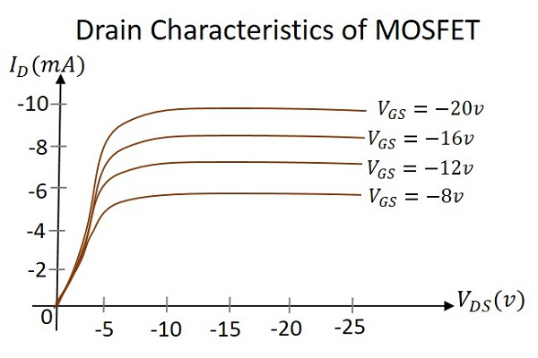
This can be better understood by having an idea on the drain characteristics curve.

Drain Characteristics

The drain characteristics of a MOSFET are drawn between the drain current IDand the drain source voltage VDS. The characteristic curve is as shown below for different values of inputs.
Drain Characteristics
Actually when VDS is increased, the drain current ID should increase, but due to the applied VGS, the drain current is controlled at certain level. Hence the gate current controls the output drain current.

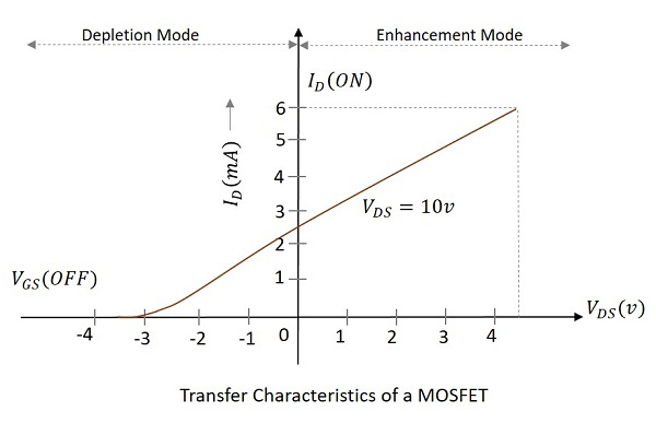
Transfer Characteristics

Transfer characteristics define the change in the value of VDS with the change in ID and VGS in both depletion and enhancement modes. The below transfer characteristic curve is drawn for drain current versus gate to source voltage.
Transfer Characteristics

Comparison between BJT, FET and MOSFET

Now that we have discussed all the above three, let us try to compare some of their properties.
TERMSBJTFETMOSFET
Device typeCurrent controlledVoltage controlledVoltage Controlled
Current flowBipolarUnipolarUnipolar
TerminalsNot interchangeableInterchangeableInterchangeable
Operational modesNo modesDepletion mode onlyBoth Enhancement and Depletion modes
Input impedanceLowHighVery high
Output resistanceModerateModerateLow
Operational speedLowModerateHigh
NoiseHighLowLow
Thermal stabilityLowBetterHigh
So far, we have discussed various electronic components and their types along with their construction and working. All of these components have various uses in the electronics field. To have a practical knowledge on how these components are used in practical circuits, please refer to the ELECTRONIC CIRCUITS tutorial.
Read More >>>.

Basic Electronics - JFET

Basic Electronics - JFET

The JFET is abbreviated as Junction Field Effect Transistor. JFET is just like a normal FET. The types of JFET are n-channel FET and P-channel FET. A p-type material is added to the n-type substrate in n-channel FET, whereas an n-type material is added to the ptype substrate in p-channel FET. Hence it is enough to discuss one type of FET to understand both.

N-Channel FET

The N-channel FET is the mostly used Field Effect Transistor. For the fabrication of Nchannel FET, a narrow bar of N-type semiconductor is taken on which P-type material is formed by diffusion on the opposite sides. These two sides are joined to draw a single connection for gate terminal. This can be understood from the following figure.
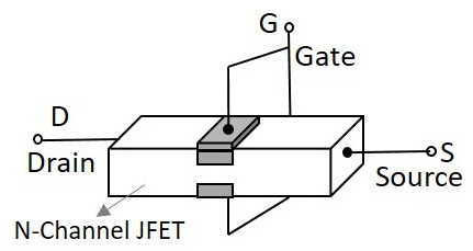
FET
These two gate depositions (p-type materials) form two PN diodes. The area between gates is called as a channel. The majority carriers pass through this channel. Hence the cross sectional form of the FET is understood as the following figure.
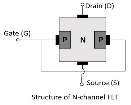
N-Channel FET
Ohmic contacts are made at the two ends of the n-type semiconductor bar, which form the source and the drain. The source and the drain terminals may be interchanged.

Operation of N-channel FET

Before going into the operation of the FET one should understand how the depletion layers are formed. For this, let us suppose that the voltage at gate terminal say VGG is reverse biased while the voltage at drain terminal say VDDis not applied. Let this be the case 1.
  • In case 1, When VGG is reverse biased and VDD is not applied, the depletion regions between P and N layers tend to expand. This happens as the negative voltage applied, attracts the holes from the p-type layer towards the gate terminal.
  • In case 2, When VDD is applied (positive terminal to drain and negative terminal to source) and VGG is not applied, the electrons flow from source to drain which constitute the drain current ID.
Let us now consider the following figure, to understand what happens when both the supplies are given.
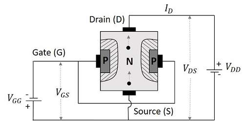
N-Channel FET Operation
The supply at gate terminal makes the depletion layer grow and the voltage at drain terminal allows the drain current from source to drain terminal. Suppose the point at source terminal is B and the point at drain terminal is A, then the resistance of the channel will be such that the voltage drop at the terminal A is greater than the voltage drop at the terminal B. Which means,
VA>VB
Hence the voltage drop is being progressive through the length of the channel. So, the reverse biasing effect is stronger at drain terminal than at the source terminal. This is why the depletion layer tends to penetrate more into the channel at point A than at point B, when both VGG and VDD are applied. The following figure explains this.
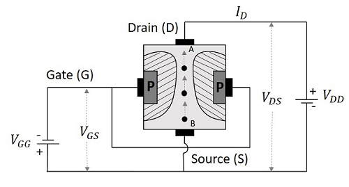
Behaviour of FET
Now that we have understood the behavior of FET, let us go through the real operation of FET.

Depletion Mode of Operation

As the width of depletion layer plays an important role in the operation of FET, the name depletion mode of operation implies. We have another mode called enhancement mode of operation, which will be discussed in the operation of MOSFETs. But JFETs have only depletion mode of operation.
Let us consider that there is no potential applied between gate and source terminals and a potential VDD is applied between drain and source. Now, a current ID flows from drain to source terminal, at its maximum as the channel width is more. Let the voltage applied between gate and source terminal VGG is reverse biased. This increases the depletion width, as discussed above. As the layers grow, the cross-section of the channel decreases and hence the drain current ID also decreases.
When this drain current is further increased, a stage occurs where both the depletion layers touch each other, and prevent the current ID flow. This is clearly shown in the following figure.
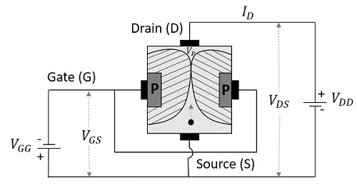
Depletion Mode
The voltage at which both these depletion layers literally “touch” is called as “Pinch off voltage”. It is indicated as VP. The drain current is literally nil at this point. Hence the drain current is a function of reverse bias voltage at gate.
Since gate voltage controls the drain current, FET is called as the voltage controlled device. This is more clearly understood from the drain characteristics curve.

Drain Characteristics of JFET

Let us try to summarize the function of FET through which we can obtain the characteristic curve for drain of FET. The circuit of FET to obtain these characteristics is given below.
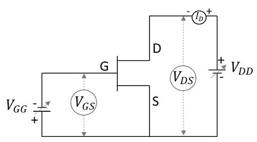
Drain Characteristics JFET
When the voltage between gate and source VGS is zero, or they are shorted, the current ID from source to drain is also nil as there is no VDS applied. As the voltage between drain and source VDS is increased, the current flow ID from source to drain increases. This increase in current is linear up to a certain point A, known as Knee Voltage.
The gate terminals will be under reverse biased condition and as ID increases, the depletion regions tend to constrict. This constriction is unequal in length making these regions come closer at drain and farther at drain, which leads to pinch off voltage. The pinch off voltage is defined as the minimum drain to source voltage where the drain current approaches a constant value (saturation value). The point at which this pinch off voltage occurs is called as Pinch off point, denoted as B.
As VDS is further increased, the channel resistance also increases in such a way that ID practically remains constant. The region BC is known as saturation region or amplifier region. All these along with the points A, B and C are plotted in the graph below.
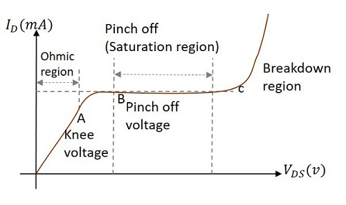
N-Channel FET Structure
The drain characteristics are plotted for drain current ID against drain source voltage VDS for different values of gate source voltage VGS. The overall drain characteristics for such various input voltages is as given under.
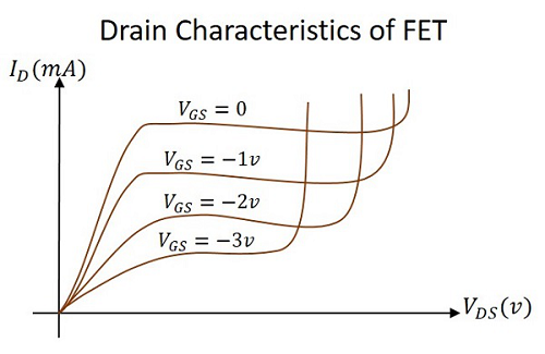
Plotted Drain Characteristics
As the negative gate voltage controls the drain current, FET is called as a Voltage controlled device. The drain characteristics indicate the performance of a FET. The drain characteristics plotted above are used to obtain the values of Drain resistance, Transconductance and Amplification Factor.

Basic Electronics - MOSFET

FETs have a few disadvantages like high drain resistance, moderate input impedance and slower operation. To overcome these disadvantages, the MOSFET which is an advanced FET is invented.
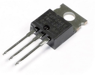
MOSFET stands for Metal Oxide Silicon Field Effect Transistor or Metal Oxide Semiconductor Field Effect Transistor. This is also called as IGFET meaning Insulated Gate Field Effect Transistor. The FET is operated in both depletion and enhancement modes of operation. The following figure shows how a practical MOSFET looks like.
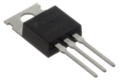
MOSFET

Construction of a MOSFET

The construction of a MOSFET is a bit similar to the FET. An oxide layer is deposited on the substrate to which the gate terminal is connected. This oxide layer acts as an insulator (sio2 insulates from the substrate), and hence the MOSFET has another name as IGFET. In the construction of MOSFET, a lightly doped substrate, is diffused with a heavily doped region. Depending upon the substrate used, they are called as P-type and N-type MOSFETs.
The following figure shows the construction of a MOSFET.
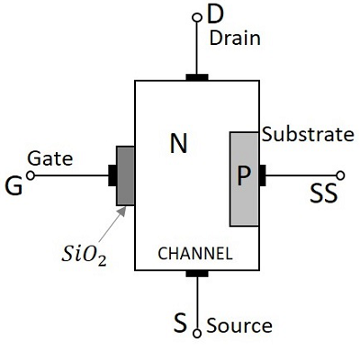
MOSFET Construction
The voltage at gate controls the operation of the MOSFET. In this case, both positive and negative voltages can be applied on the gate as it is insulated from the channel. With negative gate bias voltage, it acts as depletion MOSFET while with positive gate bias voltage it acts as an Enhancement MOSFET.

Classification of MOSFETs

Depending upon the type of materials used in the construction, and the type of operation, the MOSFETs are classified as in the following figure.
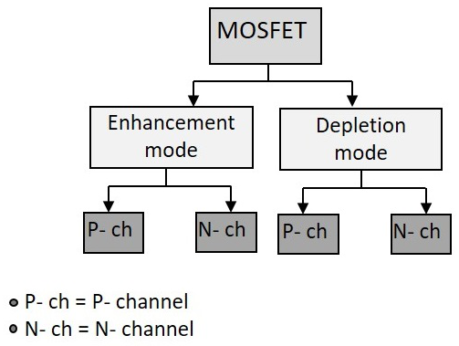
MOSFET Classification
After the classification, let us go through the symbols of MOSFET.
The N-channel MOSFETs are simply called as NMOS. The symbols for N-channel MOSFET are as given below.
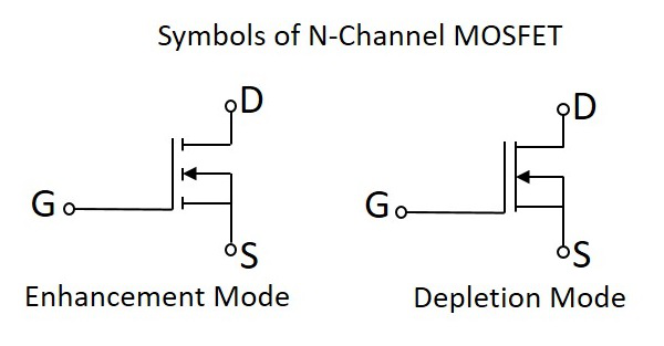
N-Channel MOSFET
The P-channel MOSFETs are simply called as PMOS. The symbols for P-channel MOSFET are as given below.
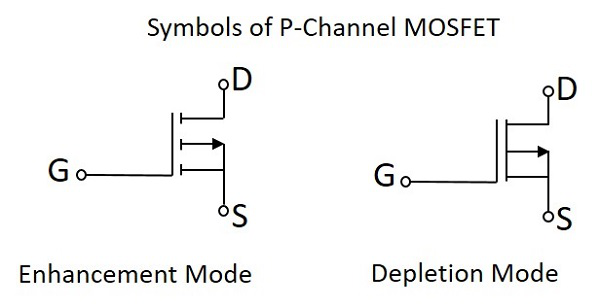
P-channel MOSFET
Now, let us go through the constructional details of an N-channel MOSFET. Usually an NChannel MOSFET is considered for explanation as this one is mostly used. Also, there is no need to mention that the study of one type explains the other too.

Construction of N- Channel MOSFET

Let us consider an N-channel MOSFET to understand its working. A lightly doped P-type substrate is taken into which two heavily doped N-type regions are diffused, which act as source and drain. Between these two N+ regions, there occurs diffusion to form an Nchannel, connecting drain and source.
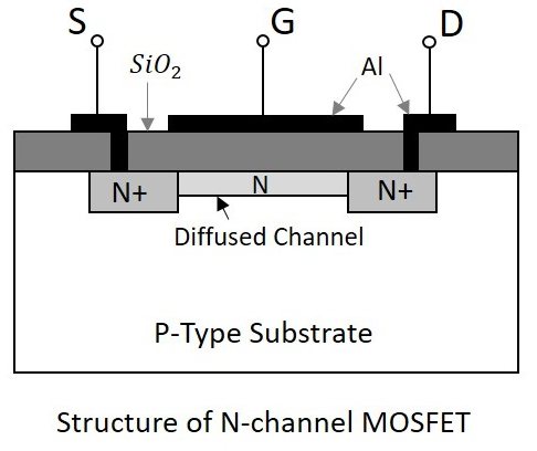
N-Channel MOSFET Construction
A thin layer of Silicon dioxide (SiO2) is grown over the entire surface and holes are made to draw ohmic contacts for drain and source terminals. A conducting layer of aluminum is laid over the entire channel, upon this SiO2layer from source to drain which constitutes the gate. The SiO2 substrate is connected to the common or ground terminals.
Because of its construction, the MOSFET has a very less chip area than BJT, which is 5% of the occupancy when compared to bipolar junction transistor. This device can be operated in modes. They are depletion and enhancement modes. Let us try to get into the details.

Working of N - Channel (depletion mode) MOSFET

For now, we have an idea that there is no PN junction present between gate and channel in this, unlike a FET. We can also observe that, the diffused channel N (between two N+ regions), the insulating dielectric SiO2 and the aluminum metal layer of the gate together form a parallel plate capacitor.
If the NMOS has to be worked in depletion mode, the gate terminal should be at negative potential while drain is at positive potential, as shown in the following figure.
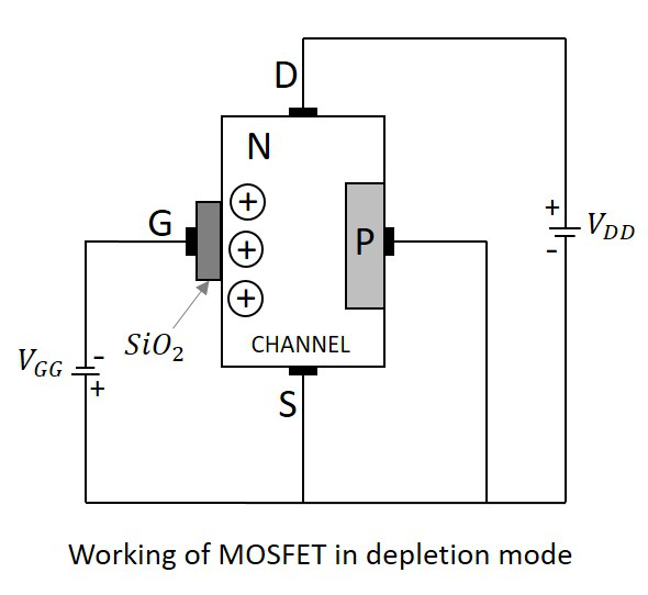
N-Channel MOSFET Working
When no voltage is applied between gate and source, some current flows due to the voltage between drain and source. Let some negative voltage is applied at VGG. Then the minority carriers i.e. holes, get attracted and settle near SiO2layer. But the majority carriers, i.e., electrons get repelled.
With some amount of negative potential at VGG a certain amount of drain current ID flows through source to drain. When this negative potential is further increased, the electrons get depleted and the current ID decreases. Hence the more negative the applied VGG, the lesser the value of drain current ID will be.
The channel nearer to drain gets more depleted than at source (like in FET) and the current flow decreases due to this effect. Hence it is called as depletion mode MOSFET.
Read More >>>.

DC Load line

DC Load line

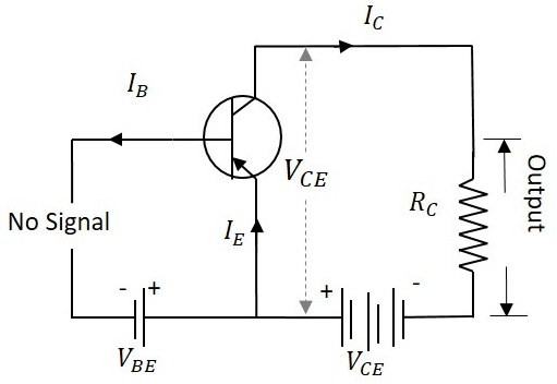
When the transistor is given the bias and no signal is applied at its input, the load line drawn at such condition, can be understood as DC condition. Here there will be no amplification as the signal is absent. The circuit will be as shown below.
DC Load Line
The value of collector emitter voltage at any given time will be
VCE=VCC−ICRC

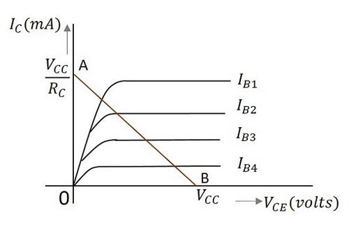
As VCC and RC are fixed values, the above one is a first degree equation and hence will be a straight line on the output characteristics. This line is called as D.C. Load line. The figure below shows the DC load line.
Characteristics
To obtain the load line, the two end points of the straight line are to be determined. Let those two points be A and B.

To obtain A

When collector emitter voltage VCE = 0, the collector current is maximum and is equal to VCC/RC. This gives the maximum value of VCE. This is shown as
VCE=VCC−ICRC

0=VCC−ICRC

IC=VCCRC

This gives the point A (OA = VCC/RC) on collector current axis, shown in the above figure.

To obtain B

When the collector current IC = 0, then collector emitter voltage is maximum and will be equal to the VCC. This gives the maximum value of IC. This is shown as
VCE=VCC−ICRC

=VCC

(As IC = 0)
This gives the point B, which means (OB = VCC) on the collector emitter voltage axis shown in the above figure.
Hence we got both the saturation and cutoff point determined and learnt that the load line is a straight line. So, a DC load line can be drawn.
The importance of this operating point is further understood when an AC signal is given at the input. This will be discussed in AMPLIFIERS tutorial.

Basic Electronics - Types of Transistors

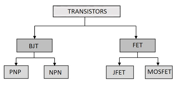
There are many types of transistors in use. Each transistor is specialized in its application. The main classification is as follows.
Transistor Types
The primary transistor is the BJT and FET is the modern version of transistor. Let us have a look at the BJTs.

Bipolar Junction Transistor

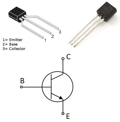
A Bipolar junction transistor, shortly termed as BJT is called so as it has two PN junctions for its function. This BJT is nothing but a normal transistor. It has got two types of configurations NPN and PNP. Usually NPN transistor is preferred for the sake of convenience. The following image shows how a practical BJT looks like.
BJT
The types of BJT are NPN and PNP transistors. The NPN transistor is made by placing a ptype material between two n-type materials. The PNP transistor is made by placing an ntype material between two p-type materials.
BJT is a current controlled device. A normal transistor which we had discussed in the previous chapters come under this category. The functionality, configurations and applications are all the same.

Field Effect Transistor

An FET is a three-terminal unipolar semiconductor device. It is a voltage controlled device unlike a bipolar junction transistor. The main advantage of FET is that it has a very high input impedance, which is in the order of Mega Ohms. It has many advantages like low power consumption, low heat dissipation and FETs are highly efficient devices. The following image shows how a practical FET looks like.
FET
The FET is a unipolar device, which means that it is made using either p-type or n-type material as main substrate. Hence the current conduction of a FET is done by either electrons or holes.

Features of FET

The following are the varied features of a Field Effect Transistor.
  • Unipolar − It is unipolar as either holes or electrons are responsible for conduction.
  • High input impedance − The input current in a FET flows due to the reverse bias. Hence it has high input impedance.
  • Voltage controlled device − As the output voltage of a FET is controlled by the gate input voltage, FET is called as the voltage controlled device.
  • Noise is low − There are no junctions present in the conduction path. Hence noise is lower than in BJTs.
  • Gain is characterized as transconductance. Transconductance is the ratio of change in output current to the change in input voltage.
  • The output impedance of a FET is low.

Advantages of FET

To prefer a FET over BJT, there should be few advantages of using FETs, rather than BJTs. Let us try to summarize the advantages of FET over BJT.
JFETBJT
It is an unipolar deviceIt is a bipolar device
Voltage driven deviceCurrent driven device
High input impedanceLow input impedance
Low noise levelHigh noise level
Better thermal stabilityLess thermal stability
Gain is characterized by transconductanceGain is characterized by voltage gain

Applications of FET

  • FET is used in circuits to reduce the loading effect.
  • FETs are used in many circuits such as Buffer Amplifier, Phase shift Oscillators and Voltmeters.

FET Terminals

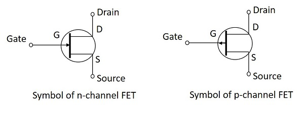
Though FET is a three terminal device, they are not the same as BJT terminals. The three terminals of FET are Gate, Source and Drain. The Source terminal in FET is analogous to the Emitter in BJT, while Gate is analogous to Base and Drain to Collector.
The symbols of a FET for both NPN and PNP types are as shown below
FET Terminals

Source

  • The Source terminal in a Field Effect Transistor is the one through which the carriers enter the channel.
  • This is analogous to the emitter terminal in a Bipolar Junction Transistor.
  • The Source terminal can be designated as S.
  • The current entering the channel at Source terminal is indicated as IS.

Gate

  • The Gate terminal in a Field Effect Transistor plays a key role in the function of FET by controlling the current through the channel.
  • By applying an external voltage at Gate terminal, the current through it can be controlled.
  • Gate is a combination of two terminals connected internally that are heavily doped.
  • The channel conductivity is said to be modulated by the Gate terminal.
  • This is analogous to the base terminal in a Bipolar Junction Transistor.
  • The Gate terminal can be designated as G.
  • The current entering the channel at Gate terminal is indicated as IG.

Drain

  • The Drain terminal in a Field Effect Transistor is the one through which the carriers leave the channel.
  • This is analogous to the collector terminal in a Bipolar Junction Transistor.
  • The Drain to Source voltage is designated as VDS.
  • The Drain terminal can be designated as D.
  • The current leaving the channel at Drain terminal is indicated as ID.

Types of FET

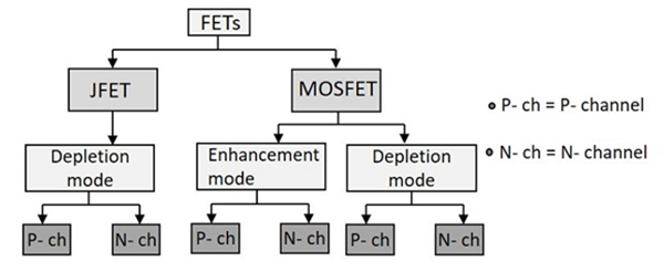
There are two main types of FETS. They are JFET and MOSFET. The following figure gives further classification of FETs.
FET Types
In the subsequent chapters, we will have a detailed discussion on JFET and MOSFET.
Read More >>>.

Activities

Latest Post

SCRIPTS

DATABASES

BIG DATA & ANALYTICS

RELATIVE ARTICLE

Learn US English

SOFT SKILLS

DIGITAL MARKETING

MICROSOFT TECHNOLOGIES

SOFTWARE QUALITY

MOBILE DEVELOPMENT

 
Support : Copyright © 2014. SUNTEC CAMPUS TUTORIAL - All Rights Reserved
Site Designed by Creating Website Inspired Support
Proudly powered by Sun Microcreators