


his tutorial supplies basic information on how to use electronic components and explains the logic behind solid state circuit design. Starting with an introduction to semiconductor physics, the tutorial moves on to cover topics such as resistors, capacitors, inductors, transformers, diodes, and transistors. Some of the topics and the circuits built with the components discussed in this tutorial are elaborately discussed in the ELECTRONIC CIRCUITS tutorial.
Audience
This tutorial should be useful for all readers who want to gain preliminary knowledge regarding the basic components used in electronic circuits.
Prerequisites
We don’t assume any prior knowledge of Electronics to understand this tutorial. The material is meant for beginners and it should be useful for most readers.
Basic Electronics - Materials
Matter is made up of molecules which consists of atoms. According to Bohr’s theory, “the atom consists of positively charged nucleus and a number of negatively charged electrons which revolve round the nucleus in various orbits”. When an electron is raised from a lower state to a higher state, it is said to be excited. While exciting, if the electron is completely removed from the nucleus, the atom is said to be ionized. So, the process of raising the atom from normal state to this ionized state is called as ionization.
The following figure shows the structure of an atom.
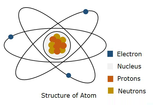
According to Bohr’s model, an electron is said to be moved in a particular Orbit, whereas according to quantum mechanics, an electron is said to be somewhere in free space of the atom, called as Orbital. This theory of quantum mechanics was proven to be right. Hence, a three dimensional boundary where an electron is probable to found is called as Atomic Orbital.
Quantum Numbers
Each orbital, where an electron moves, differs in its energy and shape. The energy levels of orbitals can be represented using discrete set of integrals and half-integrals known as quantum numbers. There are four quantum numbers used to define a wave function.
Principal Quantum number
The first quantum number that describes an electron is the Principal quantum number. Its symbol is n. It specifies the size or order (energy level) of the number. As the value of n increases, the average distance from electron to nucleus also increases, as well, the energy of the electron also increases. The main energy level can be understood as a shell.
Angular Momentum Quantum number
This quantum number has l as its symbol. This l indicates the shape of the orbital. It ranges from 0 to n-1.
l = 0, 1, 2 …n-1
For the first shell, n = 1.
i.e., for n-1, l = 0 is the only possible value of l as n = 1.
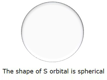
So, when l = 0, it is called as S orbital. The shape of S is spherical. The following figure represents the shape of S.
If n = 2, then l = 0, 1 as these are the two possible values for n = 2.
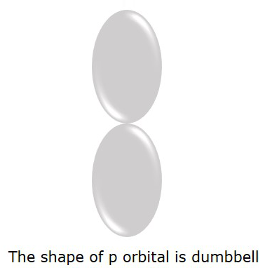
We know that it is S orbital for l = 0, but if l = 1, it is P orbital.
The P orbital where the electrons are more likely to find is in dumbbell shape. It is shown in the following figure.
Magnetic Quantum number
This quantum number is denoted by ml which represents the orientation of an orbital around the nucleus. The values of ml depend on l.
For l = 0, ml = 0 this represents S orbital.
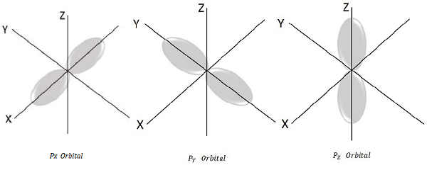
For l = 1, ml = -1, 0, +1 these are the three possible values and this represents P orbital.
Hence we have three P orbitals as shown in the following figure.
Spin Quantum number
This is represented by ms and the electron here, spins on the axis. The movement of the spinning of electron could be either clockwise or anti-clockwise as shown here under.
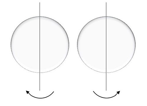
The possible values for this spin quantum number will be like,
For a movement called spin up, the result is positive half.
For a movement called spin down, the result is negative half.
These are the four quantum numbers.
Pauli Exclusion Principle
According to Pauli Exclusion Principle, no two electrons in an atom can have the same set of four identical quantum numbers. It means, if any two electrons have same values of n, s, ml (as we just discussed above) then the l value would definitely be different in them. Hence, no two electrons will have same energy.
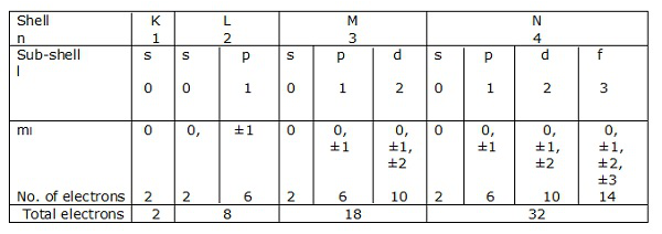
Electronic shells
If n = 1 is a shell, then l = 0 is a sub-shell.
Likewise, n = 2 is a shell, and l = 0, 1 is a sub-shell.
Shells of electrons corresponding to n = 1, 2, 3….. are represented by K, L, M, N respectively. The sub-shells or the orbitals corresponding to l = 0, 1, 2, 3 etc. are denoted by s, p, d, f etc. respectively.
Let us have a look at the electronic configurations of carbon, silicon and germanium (Group IV – A).
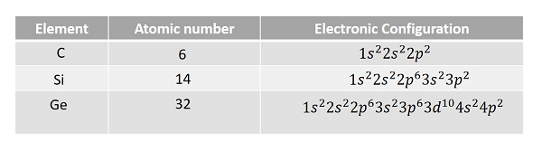
It is observed that the outermost p sub-shell in each case contains only two electrons. But the possible number of electrons is six. Hence, there are four valence electrons in each outer most shell. So, each electron in an atom has specific energy. The atomic arrangement inside the molecules in any type of substance is almost like this. But the spacing between the atoms differ from material to material.
Basic Electronics - Energy Bands
In gaseous substances, the arrangement of molecules is not close. In liquids, the molecular arrangement is moderate. But, in solids, the molecules are so closely arranged, that the electrons in the atoms of molecules tend to move into the orbitals of neighboring atoms. Hence the electron orbitals overlap when the atoms come together.
Due to the intermixing of atoms in solids, instead of single energy levels, there will be bands of energy levels formed. These set of energy levels, which are closely packed are called as Energy bands.
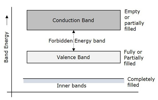
Valance Band
The electrons move in the atoms in certain energy levels but the energy of the electrons in the innermost shell is higher than the outermost shell electrons. The electrons that are present in the outermost shell are called as Valance Electrons.
These valance electrons, containing a series of energy levels, form an energy band which is called as Valence Band. The valence band is the band having the highest occupied energy.
Conduction Band
The valence electrons are so loosely attached to the nucleus that even at room temperature, few of the valence electrons leave the band to be free. These are called as free electrons as they tend to move towards the neighboring atoms.
These free electrons are the ones which conduct the current in a conductor and hence called as Conduction Electrons. The band which contains conduction electrons is called as Conduction Band. The conduction band is the band having the lowest occupied energy.
Forbidden gap
The gap between valence band and conduction band is called as forbidden energy gap. As the name implies, this band is the forbidden one without energy. Hence no electron stays in this band. The valence electrons, while going to the conduction band, pass through this.
The forbidden energy gap if greater, means that the valence band electrons are tightly bound to the nucleus. Now, in order to push the electrons out of the valence band, some external energy is required, which would be equal to the forbidden energy gap.
The following figure shows the valance band, conduction band, and the forbidden gap.
Depending upon the size of the forbidden gap, the Insulators, the Semiconductors and the Conductors are formed.
Insulators
Insulators are such materials in which the conduction cannot take place, due to the large forbidden gap. Examples: Wood, Rubber. The structure of energy bands in Insulators is as shown in the following figure.
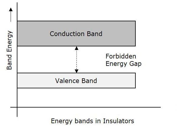
Characteristics
The following are the characteristics of Insulators.
- The Forbidden energy gap is very large.
- Valance band electrons are bound tightly to atoms.
- The value of forbidden energy gap for an insulator will be of 10eV.
- For some insulators, as the temperature increases, they might show some conduction.
- The resistivity of an insulator will be in the order of 107 ohm-meter.
Semiconductors
Semiconductors are such materials in which the forbidden energy gap is small and the conduction takes place if some external energy is applied. Examples: Silicon, Germanium. The following figure shows the structure of energy bands in semiconductors.
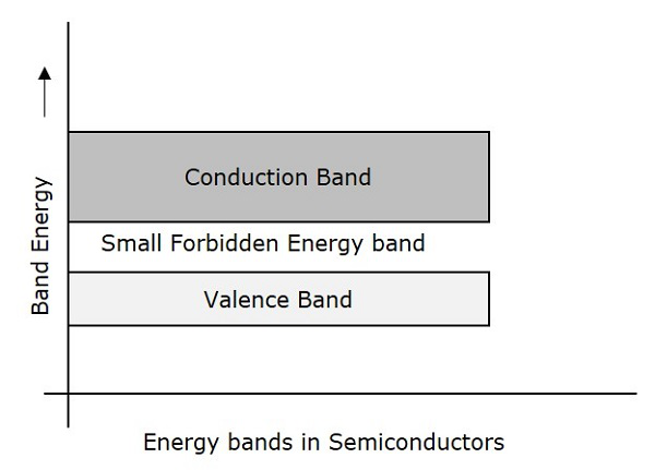
Characteristics
The following are the characteristics of Semiconductors.
- The Forbidden energy gap is very small.
- The forbidden gap for Ge is 0.7eV whereas for Si is 1.1eV.
- A Semiconductor actually is neither an insulator, nor a good conductor.
- As the temperature increases, the conductivity of a semiconductor increases.
- The conductivity of a semiconductor will be in the order of 102 mho-meter.
Conductors
Conductors are such materials in which the forbidden energy gap disappears as the valence band and conduction band become very close that they overlap. Examples: Copper, Aluminum. The following figure shows the structure of energy bands in conductors.
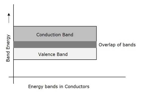
Characteristics
The following are the characteristics of Conductors.
- There exists no forbidden gap in a conductor.
- The valance band and the conduction band gets overlapped.
- The free electrons available for conduction are plenty.
- A slight increase in voltage, increases the conduction.
- There is no concept of hole formation, as a continuous flow of electrons contribute the current.
Important Terms
There is a necessity to discuss a few important terms here before we move on to subsequent chapters.
Current
It is simply the flow of electrons. A continuous flow of electrons or charged particles, can be termed as Current. It is indicated by I or i. It is measured in Amperes. This can be alternating current AC or direct current DC.
Voltage
It is the potential difference. When there occurs a difference in potentialities, between two points, there is said to be a voltage difference, measured between those two points. It is indicated by V. It is measured in Volts.
Resistance
It is the property of opposing the flow of electrons. The possession of this property can be termed as resistivity. This will be discussed later in detail.
Ohm’s Law
With the terms discussed above, we have a standard law, which is very crucial for the behavior of all the electronic components, called as Ohm’s Law. This states the relation between current and voltage in an ideal conductor.
According to Ohm’s law, the potential difference across an ideal conductor is proportional to the current through it.
An ideal conductor has no resistance. But in practice, every conductor has some resistance in it. Now, this law states that, the voltage and current are inversely proportional to the resistance it offers.
Hence, in practice, an Ohm’s law can be stated as −
According to Ohm’s law, the potential difference across a conductor is proportional to the current through it, and is inversely proportional to the resistance it offers.
This law is helpful in determining the values of unknown parameters among the three which help to analyze a circuit.
Basic Electronics - Semiconductors
A semiconductor is a substance whose resistivity lies between the conductors and insulators. The property of resistivity is not the only one that decides a material as a semiconductor, but it has few properties as follows.
- Semiconductors have the resistivity which is less than insulators and more than conductors.
- Semiconductors have negative temperature co-efficient. The resistance in semiconductors, increases with the decrease in temperature and vice versa.
- The Conducting properties of a Semiconductor changes, when a suitable metallic impurity is added to it, which is a very important property.
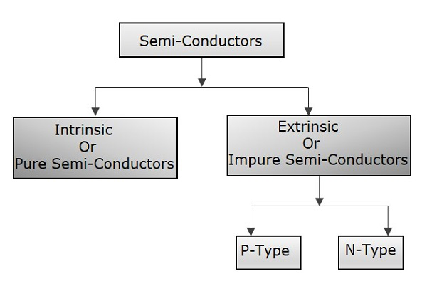
Semiconductor devices are extensively used in the field of electronics. The transistor has replaced the bulky vacuum tubes, from which the size and cost of the devices got decreased and this revolution has kept on increasing its pace leading to the new inventions like integrated electronics. The following illustration shows the classification of semiconductors.
Conduction in Semiconductors
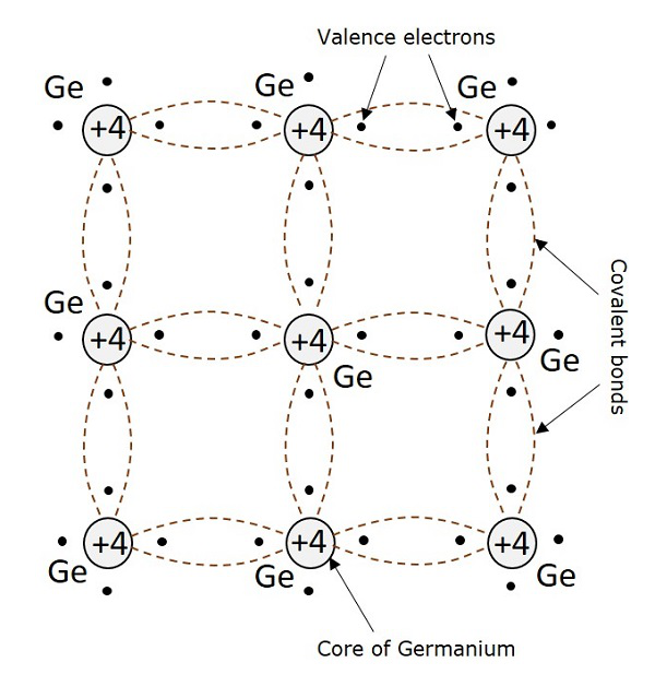
After having some knowledge on the electrons, we came to know that the outermost shell has the valence electrons which are loosely attached to the nucleus. Such an atom, having valence electrons when brought close to the other atom, the valence electrons of both these atoms combine to form “Electron pairs”. This bonding is not so very strong and hence it is a Covalent bond.
For example, a germanium atom has 32 electrons. 2 electrons in first orbit, 8 in second orbit, 18 in third orbit, while 4 in last orbit. These 4 electrons are valence electrons of germanium atom. These electrons tend to combine with valence electrons of adjoining atoms, to form the electron pairs, as shown in the following figure.
Creation of Hole
Due to the thermal energy supplied to the crystal, some electrons tend to move out of their place and break the covalent bonds. These broken covalent bonds, result in free electrons which wander randomly. But the moved away electrons creates an empty space or valence behind, which is called as a hole.
This hole which represents a missing electron can be considered as a unit positive charge while the electron is considered as a unit negative charge. The liberated electrons move randomly but when some external electric field is applied, these electrons move in opposite direction to the applied field. But the holes created due to absence of electrons, move in the direction of applied field.
Hole Current
It is already understood that when a covalent bond is broken, a hole is created. Actually, there is a strong tendency of semiconductor crystal to form a covalent bond. So, a hole doesn’t tend to exist in a crystal. This can be better understood by the following figure, showing a semiconductor crystal lattice.
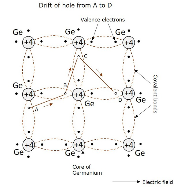
An electron, when gets shifted from a place A, a hole is formed. Due to the tendency for the formation of covalent bond, an electron from B gets shifted to A. Now, again to balance the covalent bond at B, an electron gets shifted from C to B. This continues to build a path. This movement of hole in the absence of an applied field is random. But when electric field is applied, the hole drifts along the applied field, which constitutes the hole current. This is called as hole current but not electron current because, the movement of holes contribute the current flow.
Electrons and holes while in random motion, may encounter with each other, to form pairs. This recombination results in the release of heat, which breaks another covalent bond. When the temperature increases, the rate of generation of electrons and holes increase, thus rate of recombination increases, which results in the increase of densities of electrons and holes. As a result, conductivity of semiconductor increases and resistivity decreases, which means the negative temperature coefficient.
Intrinsic Semiconductors
A Semiconductor in its extremely pure form is said to be an intrinsic semiconductor. The properties of this pure semiconductor are as follows −
- The electrons and holes are solely created by thermal excitation.
- The number of free electrons is equal to the number of holes.
- The conduction capability is small at room temperature.
In order to increase the conduction capability of intrinsic semiconductor, it is better to add some impurities. This process of adding impurities is called as Doping. Now, this doped intrinsic semiconductor is called as an Extrinsic Semiconductor.
Doping
The process of adding impurities to the semiconductor materials is termed as doping. The impurities added, are generally pentavalent and trivalent impurities.
Pentavalent Impurities
- The pentavalent impurities are the ones which has five valence electrons in the outer most orbit. Example: Bismuth, Antimony, Arsenic, Phosphorus
- The pentavalent atom is called as a donor atom because it donates one electron to the conduction band of pure semiconductor atom.
Trivalent Impurities
- The trivalent impurities are the ones which has three valence electrons in the outer most orbit. Example: Gallium, Indium, Aluminum, Boron
- The trivalent atom is called as an acceptor atom because it accepts one electron from the semiconductor atom.
Extrinsic Semiconductor
An impure semiconductor, which is formed by doping a pure semiconductor is called as an extrinsic semiconductor. There are two types of extrinsic semiconductors depending upon the type of impurity added. They are N-type extrinsic semiconductor and P-Type extrinsic semiconductor.
N-Type Extrinsic Semiconductor
A small amount of pentavalent impurity is added to a pure semiconductor to result in Ntype extrinsic semiconductor. The added impurity has 5 valence electrons.
For example, if Arsenic atom is added to the germanium atom, four of the valence electrons get attached with the Ge atoms while one electron remains as a free electron. This is as shown in the following figure.
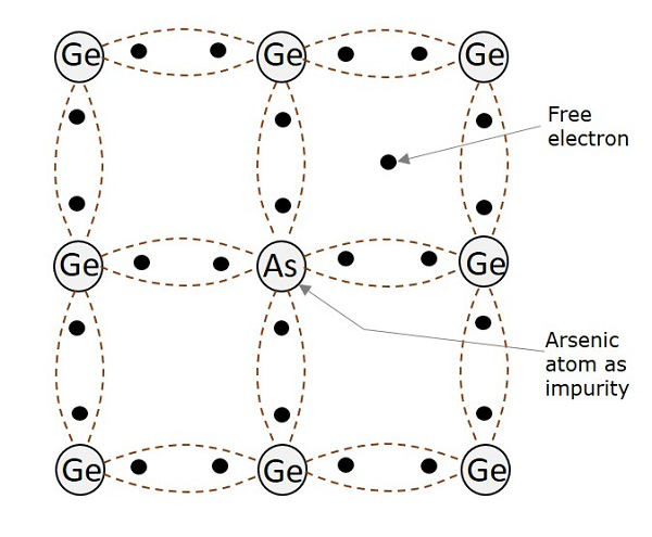
All of these free electrons constitute electron current. Hence, the impurity when added to pure semiconductor, provides electrons for conduction.
- In N-type extrinsic semiconductor, as the conduction takes place through electrons, the electrons are majority carriers and the holes are minority carriers.
- As there is no addition of positive or negative charges, the electrons are electrically neutral.
- When an electric field is applied to an N-type semiconductor, to which a pentavalent impurity is added, the free electrons travel towards positive electrode. This is called as negative or N-type conductivity.
P-Type Extrinsic Semiconductor
A small amount of trivalent impurity is added to a pure semiconductor to result in P-type extrinsic semiconductor. The added impurity has 3 valence electrons. For example, if Boron atom is added to the germanium atom, three of the valence electrons get attached with the Ge atoms, to form three covalent bonds. But, one more electron in germanium remains without forming any bond. As there is no electron in boron remaining to form a covalent bond, the space is treated as a hole. This is as shown in the following figure.
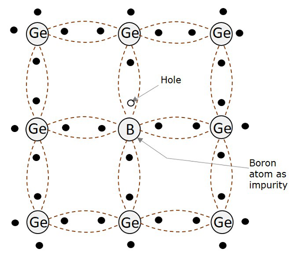
The boron impurity when added in a small amount, provides a number of holes which helps in the conduction. All of these holes constitute hole current.
- In P-type extrinsic semiconductor, as the conduction takes place through holes, the holes are majority carriers while the electrons are minority carriers.
- The impurity added here provides holes which are called as acceptors, because they accept electrons from the germanium atoms.
- As the number of mobile holes remains equal to the number of acceptors, the Ptype semiconductor remains electrically neutral.
- When an electric field is applied to a P-type semiconductor, to which a trivalent impurity is added, the holes travel towards negative electrode, but with a slow pace than electrons. This is called as P-type conductivity.
- In this P-type conductivity, the valence electrons move from one covalent bond to another, unlike N-type.
Why Silicon is Preferred in Semiconductors?
Among the semiconductor materials like germanium and silicon, the extensively used material for manufacturing various electronic components is Silicon (Si). Silicon is preferred over germanium for many reasons such as −
- The energy band gap is 0.7ev, whereas it is 0.2ev for germanium.
- The thermal pair generation is smaller.
- The formation of SiO2 layer is easy for silicon, which helps in the manufacture of many components along with integration technology.
- Si is easily found in nature than Ge.
- Noise is less in components made up of Si than in Ge.
Hence, Silicon is used in the manufacture of many electronic components, which are used to make different circuits for various purposes. These components have individual properties and particular uses.
The main electronic components include — Resistors, variable resistors, Capacitors, variable capacitors, Inductors, diodes, Tunnel diodes, Varactor diodes, Transistors, BJTs, UJTs, FETs, MOSFETs, LDR, LED, Solar cells, Thermistor, Varistor, Transformer, switches, relays, etc.
Basic Electronics - Hall Effect
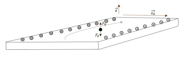
Hall Effect was named after Edwin Hall, its discoverer. This is somewhat similar to Fleming’s right hand rule. When a current carrying conductor I is placed in a transverse magnetic field B, an electric field E is induced in the conductor perpendicular to both I and B. This phenomenon is called as Hall Effect.
Explanation
When a current carrying conductor is placed in a transverse magnetic field, then this magnetic field exerts some pressure on the electrons which take a curved path to continue their journey. The conductor with energy applied is shown in the following figure. The magnetic field is also indicated.
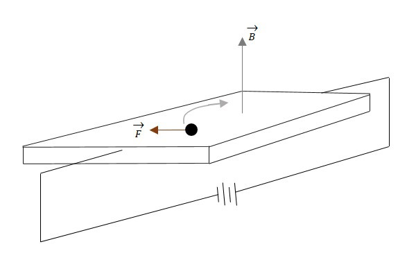
As electrons travel through the conductor that lies in a magnetic field B, the electrons will experience a magnetic force. This magnetic force will cause the electrons to travel close to one side than the other. This creates a negative charge on one side and positive charge on the other, as shown in the following figure.
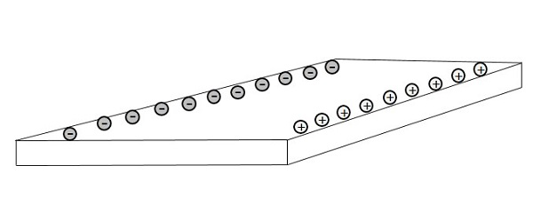
This separation of charge will create a voltage difference which is known as Hall Voltage or Hall EMF. The voltage builds up until the electric field produces an electric force on the charge that is equal and opposite of the magnetic force. This effect is known as Hall Effect.
VD is the velocity that every electron is experiencing
Since V = Ed
Where q = quantity of charge
= the magnetic field
= the drift velocity
= the Hall electric effect
d = distance between the planes in a conductor (width of the conductor)
This is the Hall EMF
Uses
The Hall Effect is used for obtaining information regarding the semiconductor type, the sign of charge carriers, to measure electron or hole concentration and the mobility. There by, we can also know whether the material is a conductor, insulator or a semiconductor. It is also used to measure magnetic flux density and power in an electromagnetic wave.
Types of Currents
Coming to the types of currents in semiconductors, there are two terms need to be discussed. They are Diffusion Current and Drift Current.
Diffusion current
When doping is done, there occurs a difference in the concentration of electrons and holes. These electrons and holes tend to diffuse from higher concentration of charge density, to lower concentration level. As these are charge carriers, they constitute a current called diffusion current.
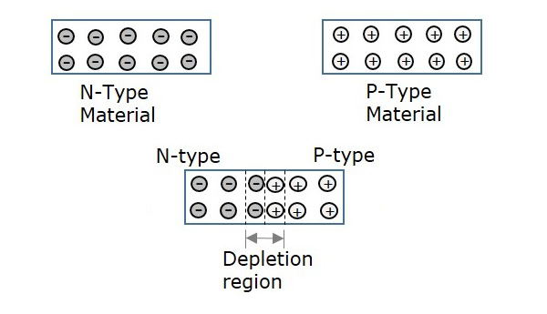
To know about this in detail, let us consider an N-type material and a P-type material.
- N-type material has electrons as majority carriers and few holes as minority carriers.
- P-type material has holes as majority carriers and few electrons as minority carriers.
If these two materials are brought too close to each other to join, then few electrons from valence band of N-type material, tend to move towards P-type material and few holes from valence band of P-type material, tend to move towards N-type material. The region between these two materials where this diffusion takes place, is called as Depletion region.
Hence, the current formed due to the diffusion of these electrons and holes, without the application of any kind of external energy, can be termed as Diffusion Current.


